Indexing Electron Diffraction Patterns (all content)
Note: DoITPoMS Teaching and Learning Packages are intended to be used interactively at a computer! This print-friendly version of the TLP is provided for convenience, but does not display all the content of the TLP. For example, any video clips and answers to questions are missing. The formatting (page breaks, etc) of the printed version is unpredictable and highly dependent on your browser.
Contents
Main pages
Additional pages
Aims
On completion of this TLP you should:
- Understand why the spots on an electron diffraction pattern appear where they do.
- Know how to index a diffraction pattern from a sample with a known lattice.
Before you start
It is strongly recommended that you read through the TLPs on Diffraction and Imaging and X-ray Diffraction before reading this TLP.
Introduction
Electrons can act as waves as well as particles; this is a consequence of quantum mechanics. A series of electrons hitting an object is exactly equivalent to a beam of electron waves hitting the object and it produces a diffraction pattern in the same way as a beam of X-rays does.
The two important differences between electron and X-ray diffraction are that (1) electrons have a much smaller wavelength than X-rays, and (2) the sample is very thin in the direction of the electron beam (of the order of 100 nm or less) - it has to be thin so that enough electrons can get through to form a diffraction pattern without being absorbed. These factors conspire to have a fortunate effect on the Ewald sphere construction (see The Ewald sphere in the Reciprocal Space TLP) and diffraction pattern:
-
The thin sample makes the reciprocal lattice points longer in the reciprocal direction corresponding to the real-space dimension in which the sample is thin:
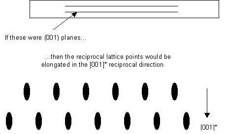
It should be noted that there is not necessarily always a particular plane oriented like this. However, it is usual for identification of crystalline phases in a sample to orient the sample so that the electron beam is parallel to a low index lattice direction, as this makes the electron diffraction pattern easier to interpret.
-
The small electron wavelength makes the radius of the Ewald sphere very large (recall its radius is 1/λ). The small electron wavelength also makes the diffraction angles θ small (1-2°); this can be seen by substituting a wavelength of 2.51 x 10⁻¹² m into the Bragg equation (see Bragg's law in the X-ray Diffraction TLP).
These make the Ewald sphere diagram look like this so that whole layers of the reciprocal lattice end up projected onto the film or screen:
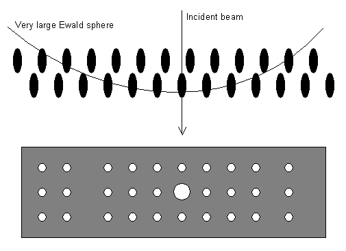
Note that the large (strong) spot in the middle is the straight-through beam (the beam which has passed through the sample without diffracting). This always has the index 000.
Caution 1: systematic (kinetic) absences appear in electron diffraction patterns just as in X-ray diffraction patterns, for the same reason: the various features of the lattice or motif diffract electrons in the same direction but the phase factors from the various features cancel, leaving an absence.
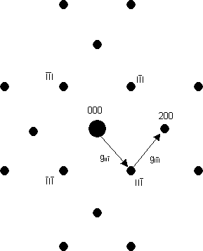
Caution 2: sometimes where there should be a systematic absence, the spot appears to be still there. This is because of the strong interaction between electrons and atoms: there is a small but significant probability that an electron will be diffracted twice, from two planes one after another - i.e. in two different reciprocal lattice directions one after another. These two directions can add up so that the twice-diffracted electron may arrive at a position in reciprocal space where there is a systematic absence. As an example, the diagram below is a schematic of the [011] electron diffraction pattern of silicon: the 200 type reflections are systematically absent. The intensity at the 200 reflections is caused by double diffraction (arising from the addition of the two reciprocal lattice vectors shown). Thus, in words, intensity can occur in the 200 reflection from, firstly, diffraction from the 11 planes, followed by, secondly, diffraction by the 11 planes as the electron wave passes through the specimen.
Mathematics relating the real space to the electron diffraction pattern
Relation 1
The distance, rhkl, on the pattern between the spot hkl and the spot 000 is related to the interplanar spacing between the hkl planes of atoms, dhkl, by the following equation: (Derivation)
\[{r_{hkl}} = \frac{{\lambda L}}{{{d_{hkl}}}}\]
where L is the distance between the sample and the film/screen.
We can therefore say that the diffraction pattern is a projection of the reciprocal lattice with projection factor λL, because reciprocal lattice vectors have length 1/dhkl.
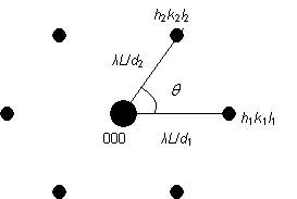
Relation 2
Since the diffraction pattern is a projection of the reciprocal lattice, the angle between the lines joining spots h1k1l1 and h2k2l2 to spot 000 is the same as the angle between the reciprocal lattice vectors [h1k1l1]* and [h2k2l2]*. This is also equal to the angle between the (h1k1l1) and (h2k2l2) planes, or equivalently the angle between the normals to the (h1k1l1) and (h2k2l2) planes. This angle is θ in the diagram below.
Using these two relations between the diffraction pattern and the reciprocal lattice, we are now able to index the electron diffraction pattern from a specimen of a known crystal structure.
The two pages linked to here refer only to indexing the central region of the diffraction pattern - the rest will be dealt with later.
Indexing with the orientation of the electron beam known
Indexing with the orientation of the electron beam unknown
Laue zones
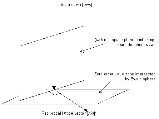
So far we have been looking at the central region of the diffraction pattern. This is only a part of the total diffraction pattern. If we look again at the Ewald sphere construction, we have:
We have been indexing the portion in the middle with the 000 spot in it. However, there are also areas of diffraction spots at the edges of the film, caused by the Ewald sphere intersecting points in an adjacent parallel plane containing reciprocal lattice points. (If the film was small or the camera length large it is possible that it did not catch these spots at the side, so that we sometimes only have the middle part.)
These outlying parts of the diffraction pattern are called Higher Order Laue Zones (HOLZs). Each of the HOLZs can be described by an equation of the general form
hu + kv + lw = N
where:
- N is always an integer, and is called the order of the Laue zone.
- [uvw] is the direction of the incident electron beam.
- hkl are the co-ordinates of an allowed reflection in the Nth order Laue zone.
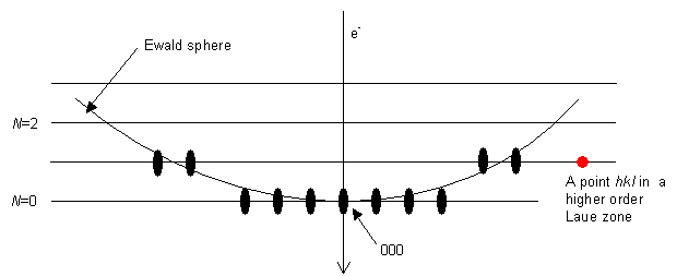
The middle part of the diffraction pattern, with 000 in it, is the zero order Laue zone (ZOLZ), because it comes from the plane for which N = 0: an allowed reflection hkl in the ZOLZ is joined to the origin 000 by a reciprocal lattice vector that lies in the ZOLZ. For the ZOLZ the electron beam [uvw] and the allowed reflection hkl satisfy the Weiss zone law hu + kv + lw = 0. The next layer up has a value N = 1, then N = 2, and so on, as shown.
From the geometry of the way in which the Ewald sphere intersects the HOLZs, the radius of the Nth HOLZ ring, Rn, in reciprocal space, is given to a very good approximation by the formula
\[{R_n} = \sqrt {\left( {\frac{{2N}}{{\lambda |uvw|}}} \right)} \]
assuming that the wavelength of the electrons is much less than the modulus |uvw| of the direction [uvw] in the crystal parallel to the electron beam direction.
Thus, HOLZs are seen more easily at lower voltages (e.g. 100 kV rather than 300 kV) and when the electron beam is parallel to a relatively high index direction in a crystal.
It is possible to index the reflections in the HOLZs on a diffraction pattern. Examples of such indexing are given in the book Transmission Electron Microscopy of Materials by D B Williams and C B Carter.
Kikuchi lines
Kikuchi lines often appear on electron diffraction patterns:
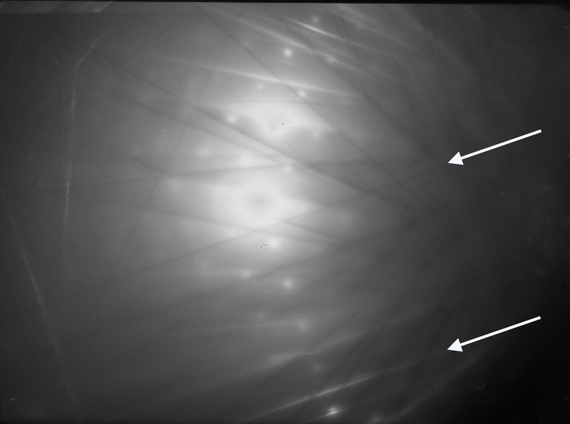
An example of a "two-beam" electron diffraction pattern with a number of Kikuchi lines. A pair
of Kikuchi lines is arrowed.
[The term "two-beam" denotes the fact that the straight-through beam, 000, and one diffraction spot are both diffracting very strongly. The intensity of all spots in this electron diffraction pattern are significantly weaker by comparison with these two beams.]
(Click on image to view larger version)
We will not learn to index the Kikuchi lines in this TLP. Instead, we will explain their origin and behaviour with the help of the following animation.
Kikuchi lines are interesting because of what they do when the crystal is moved in the beam. Diffraction spots fade or become brighter when the crystal is rotated or tilted, but stay in the same places; the Kikuchi lines move across the screen.
The difference in behaviour can be explained by the position of the effective source of the electrons that are Bragg-scattered to produce the two phenomena. The diffraction spots are produced directly from the electron beam, which either hits or misses the Bragg angle for each plane; so the spot is either present or absent depending on the orientation of the crystal. The source of the electrons that are Bragg-scattered to give Kikuchi lines is the set of inelastic scattering sites within the crystal. When the crystal is tilted the effective source of these inelastically scattered electrons is moved, but there are always still some electrons hitting a plane at the Bragg angle - they merely emerge at an angle different to the one that they did before the crystal was tilted.
Using polycrystalline materials in the TEM
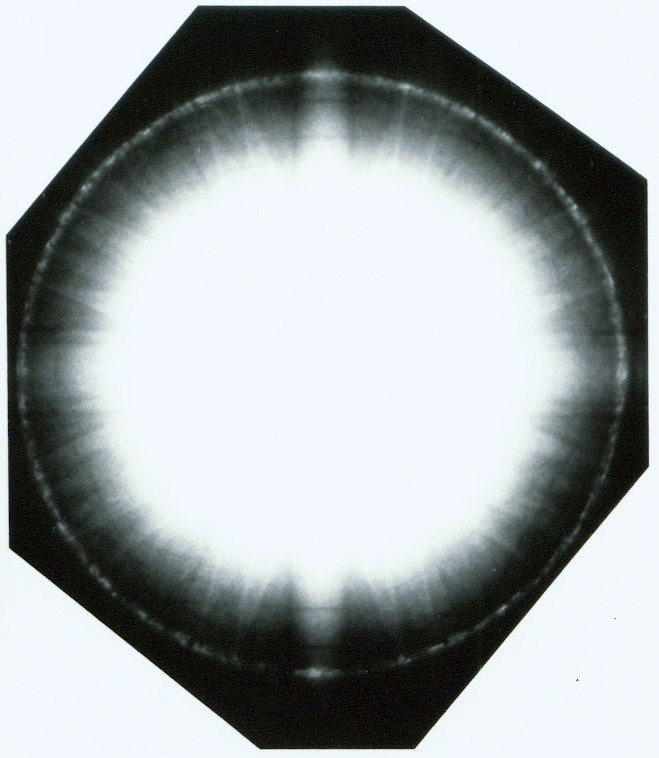
Just as with X-rays, a completely isotropic fine-grained polycrystalline sample will give a diffraction pattern of concentric rings in the zero order Laue zone (ZOLZ), as the many small crystals at random orientations produce a continuous angular distribution of hkl spots at distance 1/dhkl from the 000 spot - a ring of radius 1/dhkl around the 000 spot for each allowed reflection. The rings are then indexed according to the order of allowed reflections within the ZOLZ.
As the grain size increases, the rings within the diffraction pattern break up into discontinuous rings containing discrete reflections. If there is any texture (preferred orientation) within the specimen, arcs may be seen instead of complete rings.
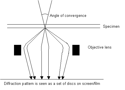
Convergent beam electron diffraction (CBED)
When a convergent beam is used instead of a parallel beam of electrons, the rays converge to a point within the specimen and come out the other side inverted like a camera. However, we do not look at the inverted image; we look at the diffraction pattern, with the spots magnified:
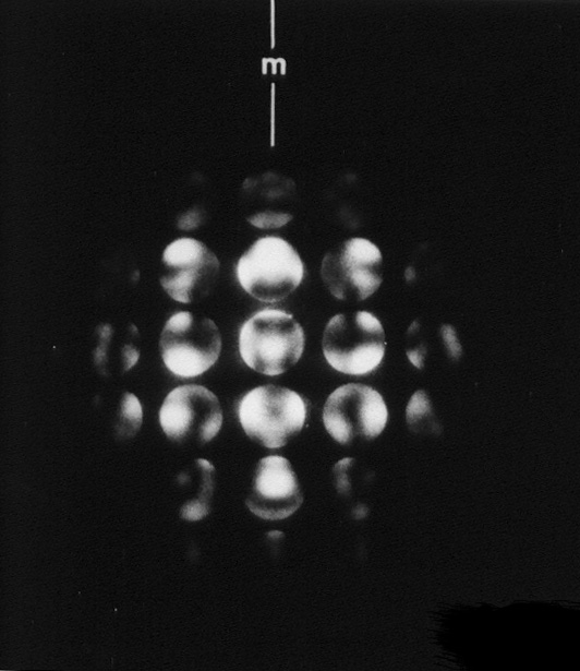
Depending on the camera length chosen, either the zero order Laue zone can be examined or the zero order Laue zone and higher order Laue zones. Two examples of CBED images are shown below. The symmetry seen is such patterns can be related to the space group symmetry of the specimen.
Examples of CBED images:
|
|
|
|
Diffraction pattern showing a zero order Laue zone |
Diffraction pattern showing a first order Laue zone |
Using other methods in conjunction with electron diffraction
Electron diffraction is a powerful technique - but other techniques must be used with it to put the results in context. This is a brief synopsis of how other methods can be used to help.
X-ray Diffraction
The majority of novel / unknown crystalline materials are indexed by single crystal X-ray diffraction methods. Originally, photographs were taken along crystallographic axes and indexing performed manually. Nowadays, data are collected with a single point or two-dimensional electronic detector and the data are indexed with automatic computer programs.
When single crystals cannot be grown, data from a polycrystalline sample may be used to determine unit cells of crystal structures. Simple structures, such as cubic crystal structures, can be indexed manually by looking for integer relationships between interplanar spacings. For more complex structures, such as orthorhombic, monoclinic and triclinic, there are several different types of computer program. However, as there is a substantial loss of information in going from single crystal diffraction data to powder diffraction data, indexing powder diffraction data is demanding. Single crystal X-ray diffraction data are the first choice.
Information from both electron and X-ray diffraction are sometimes combined to tackle difficult crystal structures. Hints from other methods maybe also be useful. Indexing X-ray reflections from both single crystals and powders also gives information about the space group of the material under investigation from considerations of symmetry and systematic absences. Measurement of accurate unit cell lattice parameters can also be undertaken - this requires high quality, high angle X-ray diffraction data.
References
[1] B.D. Cullity and S.R. Stock, 'Elements of X-ray diffraction', 3rd editon,
Prentice Hall (2001)
[2] L.S. Dent Glasser, 'Crystallography and its applications', Van Nostrand
Reinhold (1977).
[3] International Union of Crystallography website, www.iucr.org
[4] CCP 14: Available Software for Powder Diffraction Indexing including a Literature
Search List, www.ccp14.ac.uk/solution/indexing
Optical imaging
This is a very important way of analysing a specimen. Using the naked eye and optical microscopes we can determine down to a point-to-point resolution limited by the wavelength of light how many phases there are and how they relate to one another. We can also infer what type of material they are likely to be and how they may have been processed.
Chemical analysis
A wide range of chemical techniques can be used to find out what components are present in the different phases and in what proportions. This will narrow the field of possible elements that we need to consider when analysing our diffraction results. These techniques range from simple chemical tests, through infrared spectroscopy of organic samples, to a wide variety of chemical characterisation techniques that can often be performed within the transmission electron microscope.
TEM imaging
Using the TEM to image the same area of sample that is being used to produce the diffraction pattern is an invaluable technique:
|
Nitrided surface layer of austenitic stainless steel |
Diffraction pattern from nitrided surface layer of austenitic stainless steel |
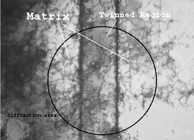
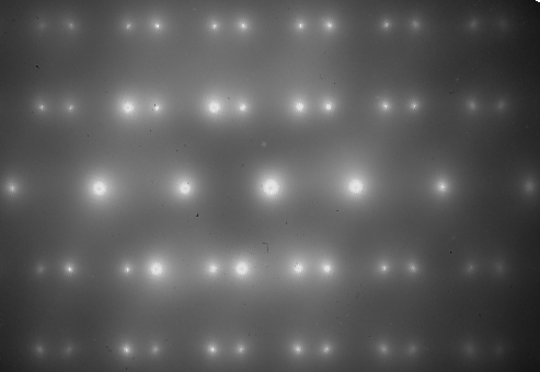
Using the image to verify that the double dots in the diffraction pattern are being caused by the two crystal structures either side of the twin boundary, we can index the pattern and determine the twin plane and the crystal structures either side of it.
Summary
In this teaching and learning package we have considered how electron diffraction patterns are formed in the transmission electron microscope. The principles of how to index spot electron diffraction patterns have been discussed in some detail. Although we have considered how to index electron diffraction patterns from relatively simple crystal structures to illustrate the basic principles, these principles are generic and can therefore be applied to any crystal structure. We have also considered other features of electron diffraction patterns such as the formation of Kikuchi lines, the formation of convergent beam electron diffraction patterns and the formation of higher index Laue zones.
Questions
Quick questions
You should be able to answer these questions without too much difficulty after studying this TLP. If not, then you should go through it again!
-
Which of the following is not an effect of the small wavelength of the electron?
-
Why might you get a diffraction spot where you thought there would be an absence?
-
Where do higher order Laue zones come from?
Deeper questions
The following questions require some thought and reaching the answer may require you to think beyond the contents of this TLP.
-
If you increase the camera length, what happens to the diffraction pattern? What about the Kikuchi lines?
-
Why would it not be possible to index a zero order Laue zone in a diffraction pattern from a cubic crystal, knowing the two points 11 and 1 ?
Open-ended questions
The following questions are not provided with answers, but intended to provide food for thought and points for further discussion with other students and teachers.
-
We have seen how electron diffraction relates to X-ray diffraction; how do you think neutron diffraction compares to electron diffraction? (Assume that we have a sufficient vacuum to enable the neutrons to reach the sample and be diffracted, and that we have some means of detecting the diffracted neutrons.)
Going further
Books
- Electron Microscopy of Thin Crystals by P B Hirsch, A Howie, R B Nicholson, D W Pashley
& M J Whelan, published by Krieger
Now out of print but explains everything very clearly. - Transmission electron microscopy of materials by D B Williams and C B Carter
This is a series of four books that contains very detailed descriptions of what happens and how to operate the microscope. Explanations are often in quantum mechanical terms and can be hard going if you want a quick reminder of how something works. - Electron microscopy and analysis by P J Goodhew, J Humphreys and R Beanland
A clear guide to the principles and phenomena involved in electron microscopy.
Derivation of rhkldhkl = λL
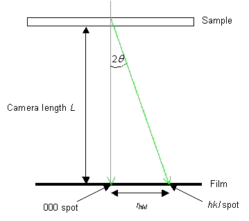
From the diagram,
\[\frac{r}{L} = \tan 2\theta \]
The Bragg condition (which is true for the sets of variables that produce diffraction spots) states that:
λ = 2dhkl sinθ
In electron diffraction, the angle θ is small so that we can make the following approximations:
tan2θ ≈ 2θ
sinθ ≈ θ
with θ in radians. Hence,
\[\frac{{{r_{hkl}}}}{L} = 2\theta = \frac{\lambda }{{{d_{hkl}}}}\]
and so it follows that
rhkldhkl = λ L
Indexing with the orientation of the electron beam known
From the Ewald sphere diagram, we know that the zero order Laue zone (ZOLZ) contains reflections hkl where hu + kv + lw = 0 (the Weiss zone law). This ZOLZ can be identified by finding two reciprocal lattice vectors in the ZOLZ. Suppose these two reciprocal lattice vectors are h1a* + k1b* + l1c* and h2a* + k2b* + l2c*. Then we know
h1u + k1v + l1w = 0
and
h2u + k2v + l2w = 0
and that the angle between these reciprocal lattice vectors is the angle between the h1k1l1 and h2k2l2 planes.
Other reflections in the electron diffraction pattern can then be deduced from simple vector addition, with the proviso that the indices of the reciprocal lattice vectors are integers and that they are not forbidden by the lattice. The pattern can then be built up manually or by computer.
Example of indexing with a known electron beam orientation
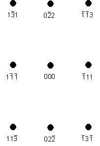
Suppose the material under examination is copper, and suppose the electron beam direction is [211]. Copper has a cubic close packed structure with a lattice parameter, a, of 0.361 nm. Allowed reflections must have h,k,l either all even or all odd. Thus the planes with the highest interplanar spacings (and hence those that give rise to reflections with the smallest rhkl values) are {111}, {200}, {220}, {311}, {222}, etc.
Looking at the {111} planes, it is apparent that the Weiss zone law is obeyed for (11) when [uvw] = [211]. Hence 11 is a possible reciprocal lattice vector.
No {200} plane will obey the Weiss zone law for [uvw] = [211], but of the {220} planes it is apparent that (02) will. Hence 02 is a second possible reciprocal lattice vector.
The angle between the 11 and 02 reciprocal lattice vectors is 90° - the dot product of these two reciprocal lattice vectors is zero. The ratio of the lengths of these two reciprocal lattice vectors is √3 : √8. These are the two shortest reciprocal lattice vectors in the [211] electron diffraction pattern. Thus the pattern looks like:
Indexing with the orientation of the electron beam unknown
If we do not know the beam orientation, it is rather more difficult to find which reciprocal plane is the one projected down onto the film.
One approach is to consult tables of angles and distance ratios for the low index reflections for the structure of the crystal we are imaging. Again, we will use copper as an example.
Table of angles
The angles in this table are the angles between the reciprocal lattice vectors given at the sides of the table in the appropriate row and column. Such a table can be extended to include planes with negative indices.
| 111 | 200 | 220 | 113 | 222 | 133 | |
| 111 | - | 54.7° | 35.3° | 29.5° | collinear | 22.0° |
| 200 | - | - | 45.0° | 72.5° | 54.7° | 76.7° |
| 220 | - | - | - | 64.7° | 35.3° | 50.0° |
| 113 | - | - | - | - | 29.5° | 26.0° |
| 222 | - | - | - | - | - | 22.0° |
| 133 | - | - | - | - | - | - |
Table of distance ratios
The dimensionless numbers in the central portion are the ratios of the 1/dhkl values for the planes given at the sides of the table (column/row).
| 1/dhkl (nm-1) | 111 | 200 | 220 | 113 | 222 | 133 | |
| 1/dhkl (nm-1) | 4.8 | 5.54 | 7.83 | 9.19 | 9.60 | 12.07 | |
| 111 | 4.8 | 1 | 1.15 | 1.63 | 1.91 | 2.00 | 2.52 |
| 200 | 5.54 | - | 1 | 1.41 | 1.66 | 1.73 | 2.18 |
| 220 | 7.83 | - | - | 1 | 1.17 | 1.22 | 1.54 |
| 113 | 9.19 | - | - | - | 1 | 1.04 | 1.31 |
| 222 | 9.60 | - | - | - | - | 1 | 1.26 |
| 133 | 12.07 | - | - | - | - | - | 1 |
When making such tables spots forbidden by the lattice type should be excluded. Thus for copper, which has an F lattice, the reflections are those with h,k,l all even or all odd.
Now we pick two spots on the diffraction pattern and measure the angle between them and the ratio of their distances from the 000 spot - and see if they correspond to any of the values in the tables.
Once we know for sure what two of the non-collinear dots are, we can index the rest of the pattern by vector addition.
Example of indexing with an unknown electron beam orientation
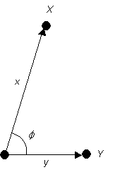
If φ were 72.5° and we were to measure the ratio x/y and find it to be numerically equal to 1.66 then we could be reasonably convinced that the dot at Y could be labelled as the 200 spot, and the dot at X could be labelled as 113. In this case our predicted electron beam direction is in the direction common to the 200 and 113 planes, i.e. [03]. This particular electron diffraction pattern has a central rectangular repeat. If this is correct, further spots on this diffraction pattern can be indexed in a self-consistent manner by vector addition.
Academic consultant: Kevin Knowles (University of Cambridge)
Content development: Jo Sharp, Andy Ball, Sarennah Longworth, Huey Hoon Hng
Photography and video: Brian Barber and Carol Best
Web development: Dave Hudson
This TLP was prepared when DoITPoMS was funded by the Higher Education Funding Council for England (HEFCE) and the Department for Employment and Learning (DEL) under the Fund for the Development of Teaching and Learning (FDTL).
Additional support for the development of this TLP came from the UK Centre for Materials Education.