Observing dislocations
A number of ways of 'seeing' dislocations in real materials have developed since the 1950s. Only in the last few years have electron microscopy techniques advanced sufficiently to allow the atomic structure around a dislocation to be resolved.
Optical microscopy - Etch pits in Sodium Chloride
Sodium chloride can be chemically etched to reveal some crystallographic features. Where a dislocation line intersects with a crystal surface, the core of the dislocation etches more rapidly than the surrounding dislocation-free crystal. This results in a small etch pit, large enough to be visible under low magnification in the optical microscope. The dislocations themselves are on the atomic scale - orders of magnitude too small to be visible with optical microscopy.
Sodium chloride single crystals can be cleaved using a razor blade tapped with a hammer. This creates a 'fresh' surface, with no environmental damage - the surface of the crystal is attacked rapidly by moisture in the air. Sodium chloride cleaves along {100} planes [link to Miller Indices]. Under the optical microscope, cleavage steps can be seen.
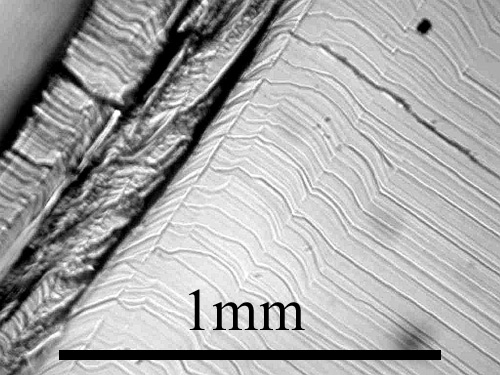
Micrograph of sodium chloride showing cleavage steps. (Click on image to view larger version.)
Dropping a few particles of silicon carbide grit onto the surface from a height of about 10 cm causes localised plastic deformation of the surface. This causes dislocations in the crystal to move. The surface can then be etched with iron (III) chloride in glacial acetic acid, and the etchant washed away with acetone. Under the optical microscope at a magnification of around 100x, 'rosettes' of etch pits may be observed, with their centres at the sites of impact of the silicon carbide. Elsewhere, more randomly distributed etch-pits may be present due to pre-existing dislocations and damage during cleaving.
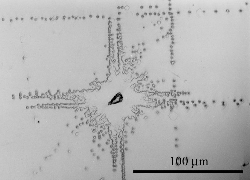
Micrograph of sodium chloride showing a rosette. (Click on image to view larger version.)
The etch pits around the deformed region are aligned along particular directions, shown schematically below:
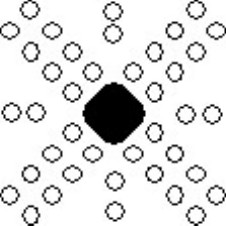
Schematic showing alignment of etch pits around deformed region.
Examining the orientation of the rosettes with respect to the surfaces of the crystal (which will be {100}) can be interpreted in terms of the slip systems in sodium chloride - that is, the direction of the Burgers vector and the slip plane on which the dislocation moves. The key point is that the dislocations only move on specific crystallographic planes in specific crystallographic directions.
More on slip systems in sodium chloride ...
Transmission electron microscopy
Dislocations can be observed in the transmission electron microscope (TEM). Due to the lattice distortion of around the core of the dislocation, some Bragg diffraction of the electron beam occurs in a localised region around the core. Intensity is therefore directed away from the 'straight through' beam, so dislocations appear as dark lines in bright field TEM images. Crystallographic information about the dislocation such as the direction of the Burgers vector can be determined from these TEM images. For some examples, see the video clips on Professor Harry Bhadeshia's website.
Being able to see dislocations as they move through a structure gives materials scientists a fascinating insight into the mechanisms of plastic deformation.
Recently, high resolution TEM has allowed microscopists to actually image the crystal planes and atomic positions within materials. The method can be exceedingly complex, making use of the phase difference between several diffracted beams caused by the atomic structure. In the example micrograph, the atomic positions in an edge dislocation in TiAl can be seen.
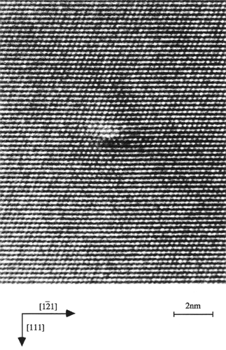
HRTEM image of a dislocation in TiAl. It is a b = ½ [10] dislocation in taken with the beam down the [10] direction. (Source: Beverly Inkson, PhD Thesis, University of Cambridge, 1994) (Click on image to view larger version.)
Scanning tunnelling microscopy (STM) is a high-resolution surface imaging technique. It allows the atomic surface structure to be deduced, revealing the disruption of the lattice at the surface where dislocation lines intersect with it.