Charge Carriers in Semiconductors
When an electric field is applied to a metal, negatively charged electrons are accelerated and carry the resulting current. In a semiconductor the charge is not carried exclusively by electrons. Positively charged holes also carry charge. These may be viewed either as vacancies in the otherwise filled valence band, or equivalently as positively charged particles.
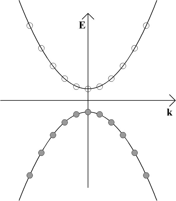
Since the Fermi-Dirac distribution is a step function at absolute zero, pure semiconductors will have all the states in the valence bands filled with electrons and will be insulators at absolute zero. This is depicted in the E-k diagram below; shaded circles represent filled momentum states and empty circles unfilled momentum states. In this diagram k, rather than k, has been used to denote that the wave vector is actually a vector, i.e., a tensor of the first rank, rather than a scalar.
If the band gap is sufficiently small and the temperature is increased from absolute zero, some electrons may be thermally excited into the conduction band, creating an electron-hole pair. This is as a result of the smearing out of the Fermi-Dirac distribution at finite temperature. An electron may also move into the conduction band from the valence band if it absorbs a photon that corresponds to the energy difference between a filled state and an unfilled state. Any such photon must have an energy that is greater than or equal to the band gap between the valence band and the conduction band, as in the diagram below.
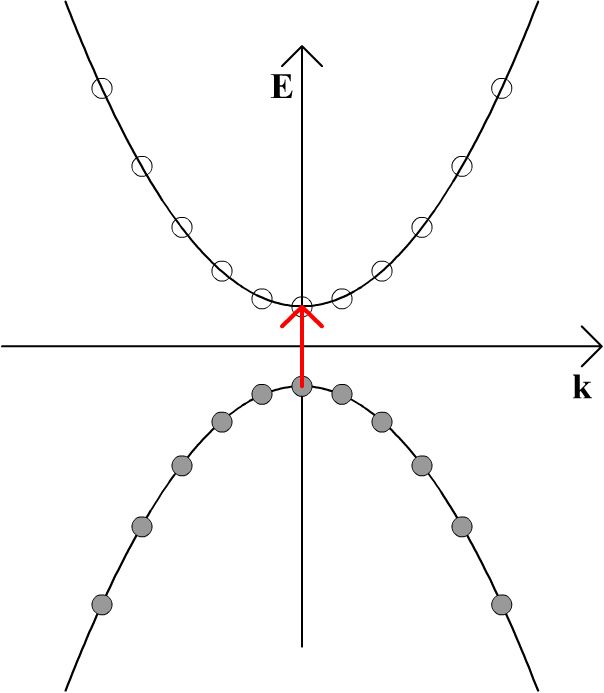
Whether thermally or photonically induced, the result is an electron in the conduction band and a vacant state in the valence band.

If an electric field is now applied to the material, all of the electrons in the solid will feel a force from the electric field. However, because no two electrons can be in the exact same quantum state, an electron cannot gain any momentum from the electric field unless there is a vacant momentum state adjacent to the state being occupied by the electron. In the above schematic, the electron in the conduction band can gain momentum from the electric field, as can an electron adjacent to the vacant state left behind in the valence band. In the diagram below, both of these electrons are shown moving to the right.
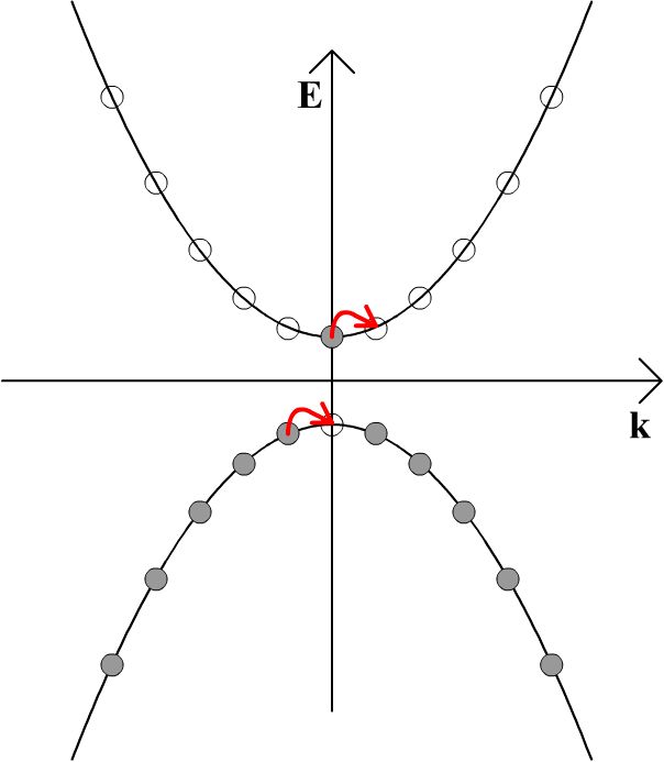
The result of this is that the electrons have some net momentum, and so there is an overall movement of charge. This slight imbalance of positive and negative momentum can be seen in the diagram below, and it gives rise to an electric current.

The vacant site in the valence band which has moved to the left can be viewed as being a particle which carries positive electric charge of equal magnitude to the electron charge. This is therefore a hole. It should be appreciated that these schematics do not represent electrons 'hopping' from site to site in real space, because the electrons are not localised to specific sites in space. These schematics are in momentum space. As such, holes should not be thought of as moving through the semiconductor like dislocations when metals are plastically deformed – it suffices to view them simply as particles which carry positive charge.
The opposite process to the creation of an electron-hole pair is called recombination. This occurs when an electron drops down in energy from the conduction band to the valence band. Just as the creation of an electron-hole pair may be induced by a photon, recombination can produce a photon. This is the principle behind semiconductor optical devices such as light-emitting diodes (LEDs), in which the photons are light of visible wavelength.