Introduction To Semiconductors
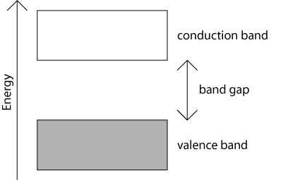
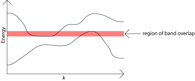
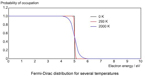
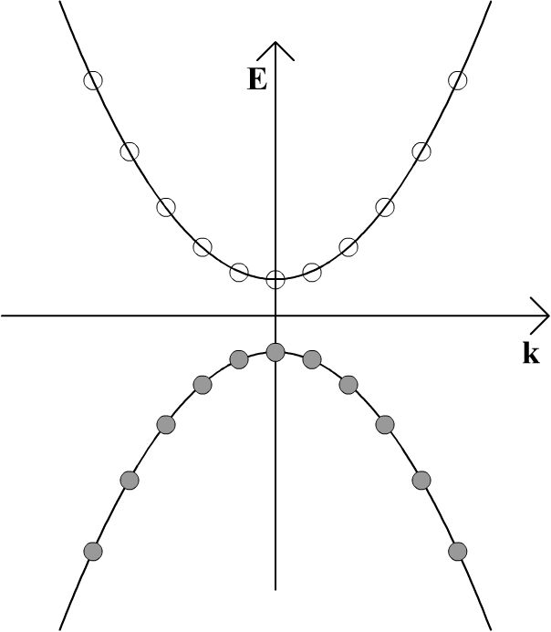
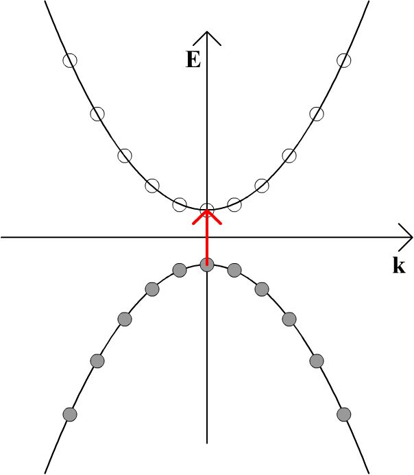
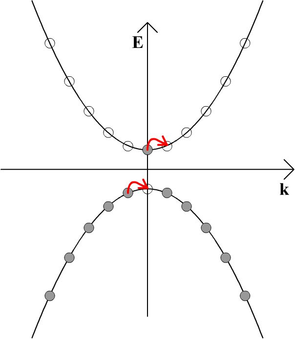
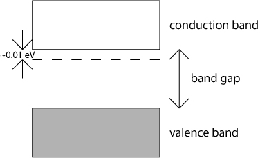
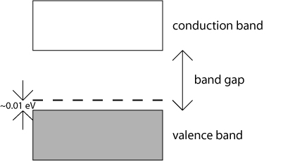
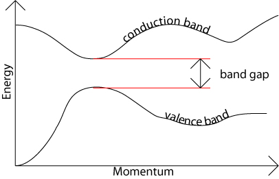
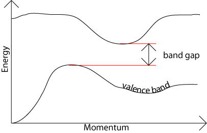
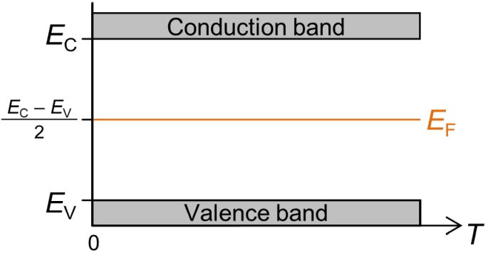
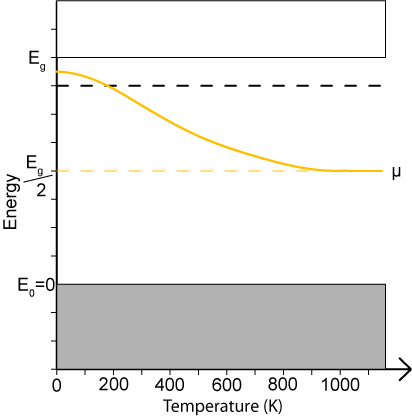
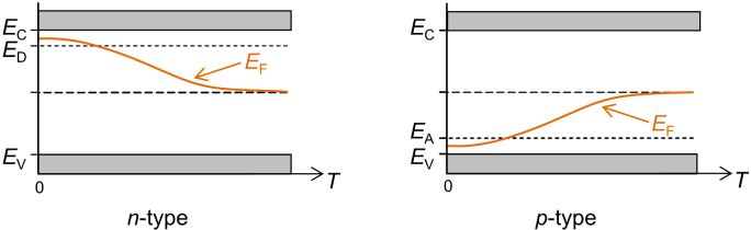
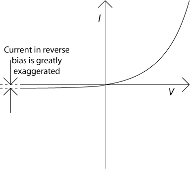
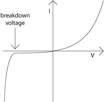
AimsBefore you startIntroductionIntroduction to Energy BandsThe Fermi–Dirac DistributionCharge Carriers in SemiconductorsIntrinsic and Extrinsic SemiconductorsDirect and Indirect Band Gap SemiconductorsCompound SemiconductorsBehaviour of the Fermi EnergyMetal–Semiconductor Junction – Rectifying ContactMetal–Semiconductor Junction – Ohmic ContactThe p–n JunctionBipolar TransistorMetal Oxide Semiconductor Field Effect Transistor (MOSFET)SummaryQuestionsGoing furtherTLP creditsTLP contentsShow all contentViewing and downloading resourcesAbout the TLPsTerms of useFeedbackCredits Print this page
Dissemination of IT for the Promotion of Materials Science (DoITPoMS)