Scanner Related Artefacts
There are a number of problems and artefacts that can arise during atomic force microscopy. This page and the following pages will discuss some of them, and how they can be overcome.
Hysteresis
The piezoelectric’s response to an applied voltage is not linear. This gives rise to hysteresis. Since the scanner makes more movement per volt at the beginning of a scan line than at the end, this can cause artefacts in the images, especially at large scan sizes. This is overcome by using a non-linear voltage waveform calculated during a calibration procedure.
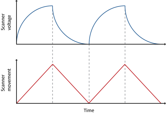
Example of a voltage waveform calibrated to overcome hysteresis
Scanner creep
If the applied voltage suddenly changes e.g. to move the scanning position, then the piezo-scanner’s response is not all at once. It moves the majority of the distance quickly, then the last part of the movement is slower. If this is done during scanning, then the slow movement will cause distortion. This is known as creep.
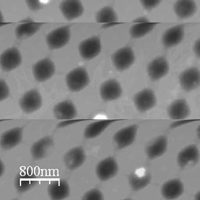
When a change in x-offset is applied, features are distorted in the x-direction
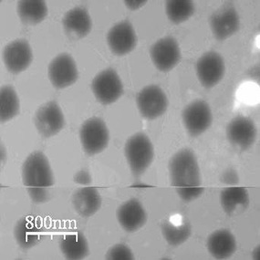
When a change in y-offset is applied, features are distorted in the y-direction
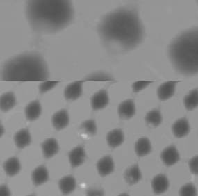
The scan size is changed abruptly, and features are distorted
Bow and tilt
Because of the construction of the piezo-scanner, the tip does not move in a perfectly flat plane. Instead its movement is in a parabolic arc, as shown in the image below. This causes the artefact known as scanner bow. Also the scanner and sample planes may not be perfectly parallel, this is known as tilt. Both of these artefacts can be removed by using post-processing software.
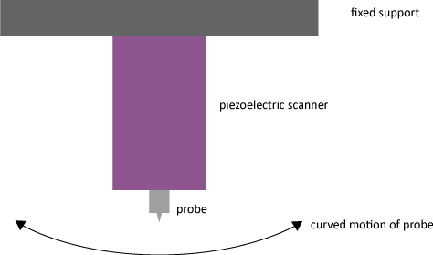
Diagram of scanner bow