Epitaxial growth
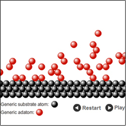
This teaching and learning package (TLP) enables you to explore the way in which perfect thin crystalline layers are deposited epitaxially (i.e. in the same crystal orientation) on semiconductor substrates. This is the way many electronic and opto-electronic devices are now fabricated using techniques such as molecular beam epitaxy (MBE).
First created: October 2011. Converted to HTML5: December 2021.