Metal–Semiconductor Junction – Rectifying Contact
Before discussing the behaviour of a metal-semiconductor boundary, it is first necessary to introduce the concept of the work function. The work function of a material is the energy required to remove an electron from the level of the chemical potential (or Fermi energy) and give it enough energy to escape to infinity and arrive there with zero energy.
Albert Einstein first proposed the concept of the work function in his work on the photoelectric effect in metals. It was for this work, rather than for his work on relativity, that Einstein was awarded the Nobel prize in 1921.
When a metal and a semiconductor are joined, two possible types of contact can result, depending on the combination of metal and semiconductor used. The contact may be rectifying, which only allows current to pass in one direction. Alternatively, it could be ohmic, in which case current can pass in either direction. Here we will discuss the rectifying contact, sometimes called the Schottky barrier contact.
The schematic below shows a metal and an n-type semiconductor. The work functions of the metal and semiconductor have been labelled φm and φs respectively. The dashed line at the top represents the zero of energy at infinity. The energy difference labelled as \( \chi \) between the bottom of the conduction band and infinity is called the electron affinity of the semiconductor.
It should be noted that the above schematic is different to the illustrations showing energy bands plotted against momentum. Any horizontal change in a diagram such as that shown above represents a variation in the energy bands with position in real space.
In the metal the electron affinity is the energy which would be released if an electron were to fall in from infinity to the highest unoccupied energy level of the material. Hence, for a metal, the electron affinity is identical to the chemical potential or Fermi energy. This is also why the electron affinity for a semiconductor is the energy difference between the bottom of the conduction band and infinity.
The schematic above is an interactive animation. By clicking the button in the bottom right hand corner, the metal and the semiconductor are brought into contact. When contact is made, electrons can move between the metal and the semiconductor. The chemical potential (or Fermi energy) can be interpreted as the free energy per electron, so because φm > φs, the electrons in the conduction band of the n-type semiconductor can lower their energy by moving from the semiconductor into the metal.
Take a moment to navigate through the whole of the animation using the buttons at the bottom of the animation. As you read further through this section, keep returning to this animation as more is gradually explained.
The flow of electrons into the metal from the semiconductor on contact in this animation causes a slight negative charging of the metal, thereby repelling further flow of electrons from the conduction band of the semiconductor into the metal. The electric potential generated by the charging of the metal causes a deformation of the energy bands in the semiconductor close to the metal-semiconductor interface. The Fermi energy in the semiconductor also falls in this region, as higher energy electrons in the region adjacent to the metal have moved into the metal. The Fermi level of the metal is not appreciably affected because there are over 1010 times more valence electrons in the metal then there are conduction electrons in the semiconductor before contact – the addition of a few extra electrons from the semiconductor clearly makes little difference to the Fermi level in the metal.
Far from the metal-semiconductor interface, the band structure in the semiconductor is unaffected except for an overall displacement down in energy. The way to think about this change in the band structure is to consider the bands in the semiconductor to be 'pinned' at the interface with the metal. The Fermi energy in the region of semiconductor immediately adjacent to the metal moves in order to be in equilibrium with the metal. This has also to be true at distances in the semiconductor remote from the interface. At a large distance from the interface, the bands therefore have the same position relative to the shifted Fermi energy as they did before the metal and semiconductor were joined.
The most immediate consequence of making contact with the metal is that a region near to the metal-semiconductor interface is produced in the semiconductor which has no conduction electrons in it – this region is depleted of electrons in the conduction band. This region is therefore called the depletion layer, or the space charge region. This region is labelled in one of the intermediate steps of the illustration.
The depletion layer acts like an energy barrier. This barrier has a height of φm − χ for electrons moving from the metal to the semiconductor. The size of the barrier for electrons moving from the semiconductor to the metal is φm − φs, which is also equal to the total downward displacement of the bands in the semiconductor remote from the metal-semiconductor interface.
At a particular finite temperature, there will be electrons in the metal that can be thermally excited enough to overcome the energy barrier and diffuse into the semiconductor conduction band. Likewise, there will be electrons in the conduction band that will have enough thermal energy to diffuse from the semiconductor into the metal. In equilibrium these currents must be equal. If they were not, charging would occur at the interface and the band structure would be deformed until the diffusion currents of the electrons were identical in both directions. The higher energy barrier encountered in moving from the metal to the semiconductor is compensated for by the much larger numbers of free electrons in the metal.
In addition to the above diffusion current, there is also a drift current. The drift current is usually very small, and independent of the height of the energy barrier. It arises through the formation of electron-hole pairs in, or very near to, the depletion layer as a result of thermal excitation. The electron in such an electron-hole pair will be accelerated into the semiconductor (electrons 'roll' downhill), while the hole will be accelerated towards the boundary with the metal (holes 'float up' to the highest point). This contribution to the current is usually very small, and is dependent on the band gap of the semiconductor and the temperature. The total current across the junction is the net sum of the diffusion current and the drift current. At equilibrium, i.e. zero externally applied voltage, the net sum of these two currents is zero.
It should be noted that any hole created in the semiconductor near the metal, as a result of the thermal excitation of electrons into the conduction band, which then reaches the boundary with the metal successfully, will ultimately be destroyed by recombining with an electron from the metal.
If the metal is now connected to the negative terminal of a battery, and the semiconductor is connected to the positive terminal, there will be a greater negative charge on the metal, and the bands in the semiconductor will be further deformed.
This will increase the energy barrier and also the width of the depletion layer. This results in the diffusion current in both directions becoming negligible, because the energy barrier is large for both directions of diffusion. The contribution from the drift current will still remain, producing an extremely small and constant current of electrons from the metal into the positively biased semiconductor. This situation is called reverse bias.
When the metal is connected instead to the positive terminal of a battery, the negative charge on the metal is slightly reduced, and this will in turn reduce the deformation of the bands in the semiconductor. The resulting reduction in the width of the depletion layer, and the much lower energy barrier for electrons to move from the semiconductor into the metal results in a large net movement of electrons into the metal from the semiconductor, and therefore a net current flow. This is called forward bias.
If you have not already done so, take another look through the animation earlier in this section.
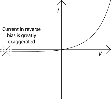
The overall current–voltage characteristic for a rectifying contact of this type is shown in the figure below. Note that the size of the current for reverse bias (negative voltage) has been greatly exaggerated.
A similar rectifying device can also be made from the junction of a p-type semiconductor with a metal. In this case, φm has to be smaller than φs to form a rectifying contact. This can be represented schematically in a manner similar to that shown above for the n-type semiconductor–metal case. The animation below depicts the situation for a p-type semiconductor–metal rectifying contact.
The major difference here is that the sign of the voltage is reversed for a p-type device, i.e., it passes current when the metal is connected to the negative terminal, and blocks current when it is connected to the positive terminal.
Rectifying contacts can also be made from a junction between n-type and p-type semiconducting materials. Such a contact is termed a p–n junction and is discussed in the section of this TLP entitled The p–n Junction.