Introduction To Semiconductors (all content)
Note: DoITPoMS Teaching and Learning Packages are intended to be used interactively at a computer! This print-friendly version of the TLP is provided for convenience, but does not display all the content of the TLP. For example, any video clips and answers to questions are missing. The formatting (page breaks, etc) of the printed version is unpredictable and highly dependent on your browser.
Contents
Aims
On completion of this TLP you should:
- Be familiar with the concept of energy bands;
- Understand about the two charge carriers, electrons and holes, in semiconductors;
- Understand why doping of semiconductors is useful;
- Be familiar with basic electronic devices made using semiconductors and how these devices operate.
Before you start
It is advisable before attempting this TLP to ensure familiarity with the simple theory of covalent chemical bonding.
Introduction
Semiconductors are amongst the most technologically important materials in existence today. With the exception of extremely simple objects such as filament light bulbs, all of the electronic devices that we use involve some semiconductor-based devices.
In order to appreciate how semiconductors can be used to create devices, it is important to have an understanding of the basic electronic properties of semiconductors. The first section of this TLP will concentrate on describing what it is that makes a material a semiconductor, and how semiconductors respond to an applied electric field. The second half of the TLP gives some specific examples of semiconductor devices and where these devices are used.
Introduction to Energy Bands
When two valence electron atomic orbitals in a simple molecule such as hydrogen combine to form a chemical bond, two possible molecular orbitals result. One molecular orbital is lowered in energy relative to the sum of the energies of the individual electron orbitals, and is referred to as the 'bonding' orbital. The other molecular orbital is raised in energy relative to the sum of the energies of the individual electron orbitals and is termed the 'anti-bonding' orbital.
In a solid, the same principles apply. If N valence electron atomic orbitals, all of the same energy, are taken and combined to form bonds, N possible energy levels will result. Of these, N/2 will be lowered in energy and N/2 will be raised in energy with respect to the sum of the energies of the N valence electron atomic orbitals.
However, instead of forming N/2 bonding levels all of the exact same energy, the allowed energy levels will be smeared out into energy bands. Within these energy bands local differences between energy levels are extremely small. The energy differences between the levels within the bands are much smaller than the difference between the energy of the highest bonding level and the energy of the lowest anti-bonding level. Like molecular orbitals, and also atomic orbitals, each energy level can contain at most two electrons of opposite spin.
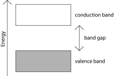
The allowed energy levels are so close together that they are sometimes considered as being continuous. It is very important to bear in mind that, while this is a useful and reasonable approximation in some calculations, the bands are actually composed of a finite number of very closely spaced electron energy levels.
If there is one electron from each atom associated with each of the N orbitals that are combined to form the bands, then because each resulting energy level can be doubly occupied, the 'bonding' band, or valence band will be completely filled and the 'anti-bonding' band, or conduction band will be empty. This is depicted schematically in the picture above by the grey shading of the valence band.
Electrons cannot have any values of energy that lie outside these bands. An electron can only move ('be promoted') from the valence band to the conduction band if it is given an energy at least as great as the band gap energy. This can happen if, for example, the electron were to absorb a photon of sufficiently high energy.
If, as in the above one-dimensional schematic, a band is completely filled with electrons, and the band immediately above it is empty, the material has an energy band gap. This band gap is the energy difference between the highest occupied state in the valence band and the lowest unoccupied state in the conduction band. The material is either a semiconductor if the band gap is relatively small, or an insulator if the band gap is relatively large.
Electrons in metals are also arranged in bands, but in a metal the electron distribution is different - electrons are not localised on individual atoms or individual bonds. In a simple metal with one valence electron per atom, such as sodium, the valence band is not full, and so the highest occupied electron states lie some distance from the top of the valence band. Such materials are good electrical conductors, because there are empty energy states available just above the highest occupied states, so that electrons can easily gain energy from an applied electric field and jump into these empty energy states.
The distinction between an insulator and a semiconductor is less precise. In general, a material with a band gap of less than about 3 eV is regarded as a semiconductor. A material with a band gap of greater than 3 eV will commonly be regarded as an insulator. A number of ceramics such as silicon carbide (SiC), titanium dioxide (TiO2), barium titanate (BaTiO3) and zinc oxide (ZnO) have band gaps around 3 eV and are regarded by ceramicists as semiconductors. Such ceramics are often referred to as wide-band-gap semicondutors.
The distinction between semiconductors and insulators arises because in small band gap materials at room temperature a small, but appreciable, number of electrons can be excited from the filled valence bands into the unfilled conduction bands simply by thermal vibration. This leads to semiconducting materials having electrical conductivities between those of metals and those of insulators.
The picture we have sketched here is only a very simple qualitative picture of the electronic structure of a semiconductor designed to capture essential aspects of the band structure in semiconductors relevant to this TLP. More precise and quantitative approaches exist - see Going Further. Such quantitative approaches are generally quite complex and require an understanding of quantum mechanics. Fortunately, the very simple qualitative picture described above for semiconductors is all that we need to be able to build upon and develop in this TLP.
An extension of the simple band energy diagram with only the vertical axis labelled as energy, with the horizontal axis unlabelled, is to plot the energy vertically against wave vector, k. From de Broglie's relationship p = k where p is momentum and is Planck's constant, h, divided by 2π. Such plots therefore relate energy to momentum. The reason why such plots are useful lies in the more quantitative methods referred to above, from which we shall simply quote useful results.
The energy of a classical, non-quantum, particle is proportional to the square of its momentum. This is also true for a free electron, as in the most simple picture possible of valence electrons in metals where the electrostatic potential from the nuclei is ignored. However, in a real crystalline solid the periodicity of the lattice and the electrostatic potential from the nuclei together mean that in the quantum world in a crystalline material the electron energy, E, is not simply proportional to the square of the momentum, and so is not proprtional to the square of the wave vector, k.
In these E-k diagrams, often called band diagrams, plotted in what is referred to as a reduced zone scheme, the momentum that is plotted is actually a quantity called crystal momentum. The distinction between momentum and crystal momentum arises from the periodicity of the solid. Fortunately, this distinction is not important for understanding this TLP on semiconductors.
There are usually many different values of electron energy possible for any given value of the electron momentum. Each possible energy value lies in one of the energy bands.
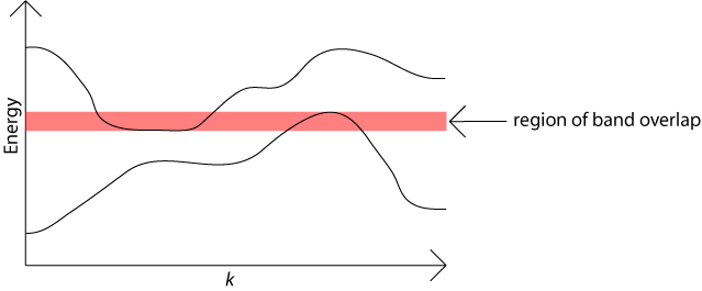
When plotted against the wave vector, k, the bands of allowed energy are not really flat. This means that bands can overlap in energy, as the maximum value in one band may be higher then the minimum value in another band. In this case the relevant maximum and minimum will occur for different values of k because energy bands never cross over each other. This is one way in which metals can have partially filled energy bands. The available energy states are filled with electrons starting with those lowest in energy. Such overlapping of bands as a function of k does not occur in semiconductors.
The Fermi–Dirac Distribution
Electrons are an example of a type of particle called a fermion. Other fermions include protons and neutrons. In addition to their charge and mass, electrons have another fundamental property called spin. A particle with spin behaves as though it has some intrinsic angular momentum. This causes each electron to have a small magnetic dipole. The spin quantum number is the projection along an arbitrary axis (usually referred to in textbooks as the z-axis) of the spin of a particle expressed in units of . Electrons have spin ½, which can be aligned in two possible ways, usually referred to as 'spin up' or 'spin down'.
All fermions have half-integer spin. A particle that has integer spin is called a boson. Photons, which have spin 1, are examples of bosons. A consequence of the half-integer spin of fermions is that this imposes a constraint on the behaviour of a system containing more then one fermion.
This constraint is the Pauli exclusion principle, which states that no two fermions can have the exact same set of quantum numbers. It is for this reason that only two electrons can occupy each electron energy level – one electron can have spin up and the other can have spin down, so that they have different spin quantum numbers, even though the electrons have the same energy.
These constraints on the behaviour of a system of many fermions can be treated statistically. The result is that electrons will be distributed into the available energy levels according to the Fermi Dirac Distribution:
\[f\left( E \right) = \frac{1}{{\exp \left( {\left( {E - \mu } \right)/{k_{\rm{B}}}T} \right) + 1}}\]
where \( f\left( E \right) \) is the occupation probability of a state of energy \( E \), \( k_{\rm{B}} \) is Boltzmann's constant, \( \mu \) (the Greek letter mu) is the chemical potential, and \( T \) is the temperature in Kelvin.
The distribution describes the occupation probability for a quantum state of energy \( E \) at a temperature \( T \). If the energies of the available electron states and the degeneracy of the states (the number of electron energy states that have the same energy) are both known, this distribution can be used to calculate thermodynamic properties of systems of electrons.
At absolute zero the value of the chemical potential, \( \mu \), is defined as the Fermi energy. At room temperature the chemical potential for metals is virtually the same as the Fermi energy – typically the difference is only of the order of 0.01%. Not surprisingly, the chemical potential for metals at room temperature is often taken to be the Fermi energy. For a pure undoped semiconductor at finite temperature, the chemical potential always lies halfway between the valence band and the conduction band. However, as we shall see in a subsequent section of this TLP, the chemical potential in extrinsic (doped) semiconductors has a significant temperature dependence.
In order to understand the behaviour of electrons at finite temperature qualitatively in metals and pure undoped semiconductors, it is clearly sufficient to treat \( \mu \) as a constant to a first approximation. With this approximation, the Fermi-Dirac distribution can be plotted at several different temperatures. In the figure below, \( \mu \) was set at 5 eV.
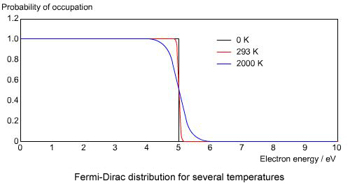
From this figure it is clear that at absolute zero the distribution is a step function. It has the value of 1 for energies below the Fermi energy, and a value of 0 for energies above. For finite temperatures the distribution gets smeared out, as some electrons begin to be thermally excited to energy levels above the chemical potential, \( \mu \). The figure shows that at room temperature the distribution function is still not very far from being a step function.
Charge Carriers in Semiconductors
When an electric field is applied to a metal, negatively charged electrons are accelerated and carry the resulting current. In a semiconductor the charge is not carried exclusively by electrons. Positively charged holes also carry charge. These may be viewed either as vacancies in the otherwise filled valence band, or equivalently as positively charged particles.
Since the Fermi-Dirac distribution is a step function at absolute zero, pure semiconductors will have all the states in the valence bands filled with electrons and will be insulators at absolute zero. This is depicted in the E-k diagram below; shaded circles represent filled momentum states and empty circles unfilled momentum states. In this diagram k, rather than k, has been used to denote that the wave vector is actually a vector, i.e., a tensor of the first rank, rather than a scalar.
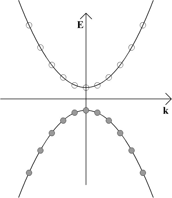
If the band gap is sufficiently small and the temperature is increased from absolute zero, some electrons may be thermally excited into the conduction band, creating an electron-hole pair. This is as a result of the smearing out of the Fermi-Dirac distribution at finite temperature. An electron may also move into the conduction band from the valence band if it absorbs a photon that corresponds to the energy difference between a filled state and an unfilled state. Any such photon must have an energy that is greater than or equal to the band gap between the valence band and the conduction band, as in the diagram below.
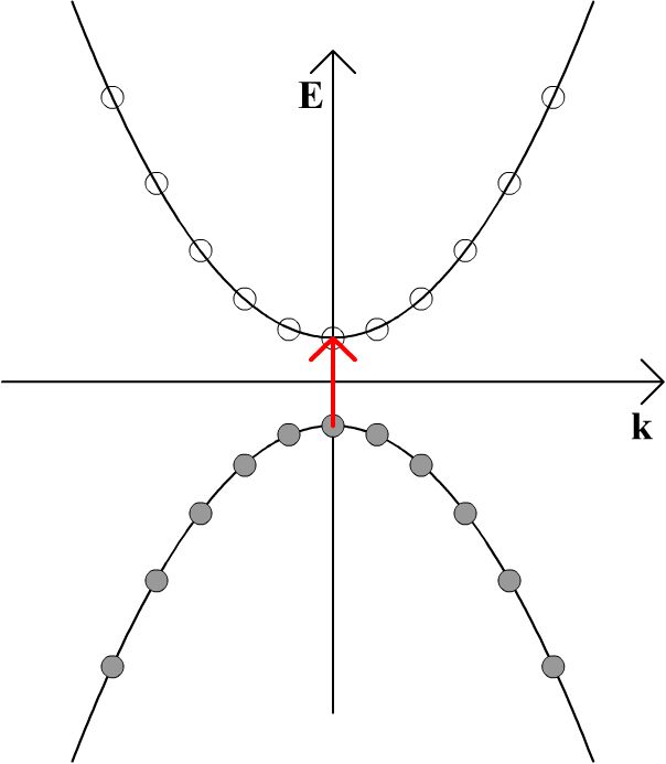
Whether thermally or photonically induced, the result is an electron in the conduction band and a vacant state in the valence band.

If an electric field is now applied to the material, all of the electrons in the solid will feel a force from the electric field. However, because no two electrons can be in the exact same quantum state, an electron cannot gain any momentum from the electric field unless there is a vacant momentum state adjacent to the state being occupied by the electron. In the above schematic, the electron in the conduction band can gain momentum from the electric field, as can an electron adjacent to the vacant state left behind in the valence band. In the diagram below, both of these electrons are shown moving to the right.
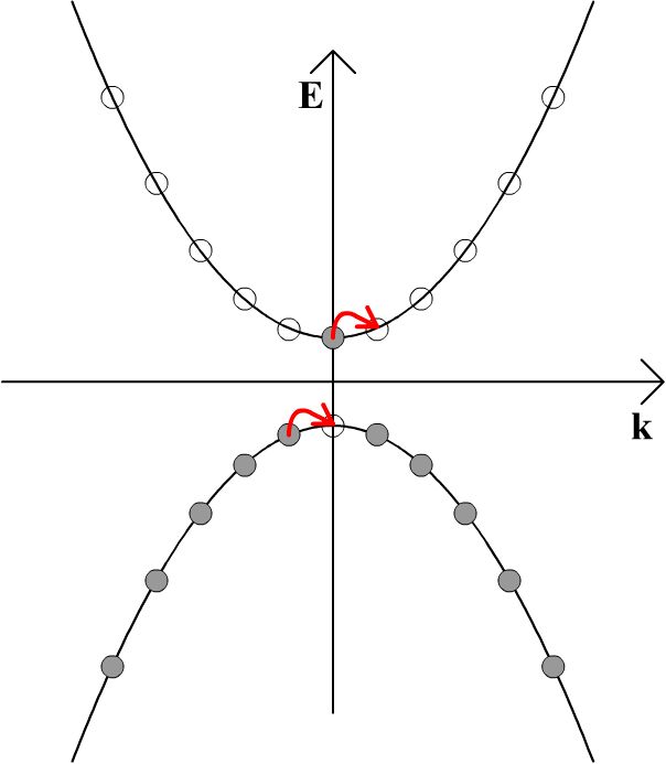
The result of this is that the electrons have some net momentum, and so there is an overall movement of charge. This slight imbalance of positive and negative momentum can be seen in the diagram below, and it gives rise to an electric current.

The vacant site in the valence band which has moved to the left can be viewed as being a particle which carries positive electric charge of equal magnitude to the electron charge. This is therefore a hole. It should be appreciated that these schematics do not represent electrons 'hopping' from site to site in real space, because the electrons are not localised to specific sites in space. These schematics are in momentum space. As such, holes should not be thought of as moving through the semiconductor like dislocations when metals are plastically deformed – it suffices to view them simply as particles which carry positive charge.
The opposite process to the creation of an electron-hole pair is called recombination. This occurs when an electron drops down in energy from the conduction band to the valence band. Just as the creation of an electron-hole pair may be induced by a photon, recombination can produce a photon. This is the principle behind semiconductor optical devices such as light-emitting diodes (LEDs), in which the photons are light of visible wavelength.
Intrinsic and Extrinsic Semiconductors
In most pure semiconductors at room temperature, the population of thermally excited charge carriers is very small. Often the concentration of charge carriers may be orders of magnitude lower than for a metallic conductor. For example, the number of thermally excited electrons cm–3 in silicon (Si) at 298 K is 1.5 × 10¹⁰. In gallium arsenide (GaAs) the population is only 1.1 × 10⁶ electrons cm–3. This may be compared with the number density of free electrons in a typical metal, which is of the order of 1028 electrons cm–3.
Given these numbers of charge carriers, it is no surprise that, when they are extremely pure, silicon and other semiconductors have high electrical resistivities, and therefore low electrical conductivities. This problem can be overcome by doping a semiconducting material with impurity atoms. Even very small controlled additions of impurity atoms at the 0.0001% level can make very large differences to the conductivity of a semiconductor.
It is easiest to begin with a specific example. Silicon is a group IV element, and has 4 valence electrons per atom. In pure silicon the valence band is completely filled at absolute zero. At finite temperatures the only charge carriers are the electrons in the conduction band and the holes in the valence band that arise as a result of the thermal excitation of electrons to the conduction band. These charge carriers are called intrinsic charge carriers, and necessarily there are equal numbers of electrons and holes. Pure silicon is therefore an example of an intrinsic semiconductor.
If a very small number of atoms of a group V element such as phosphorus (P) are added to the silicon as substitutional atoms in the lattice, additional valence electrons are introduced into the material because each phosphorus atom has 5 valence electrons. These additional electrons are bound only weakly to their parent impurity atoms (the bonding energies are of the order of hundredths of an eV), and even at very low temperatures these electrons can be promoted into the conduction band of the semiconductor. This is often represented schematically in band diagrams by the addition of 'donor levels' just below the bottom of the conduction band, as in the schematic below.
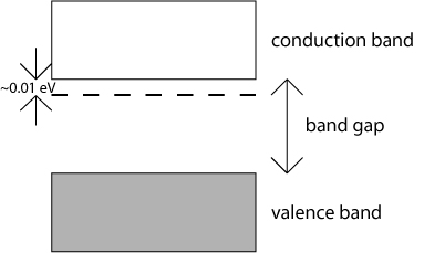
The presence of the dotted line in this schematic does not mean that there now exist allowed energy states within the band gap. The dotted line represents the existence of additional electrons which may be easily excited into the conduction band. Semiconductors that have been doped in this way will have a surplus of electrons, and are called n-type semiconductors. In such semiconductors, electrons are the majority carriers.
Conversely, if a group III element, such as aluminium (Al), is used to substitute for some of the atoms in silicon, there will be a deficit in the number of valence electrons in the material. This introduces electron-accepting levels just above the top of the valence band, and causes more holes to be introduced into the valence band. Hence, the majority charge carriers are positive holes in this case. Semiconductors doped in this way are termed p-type semiconductors.
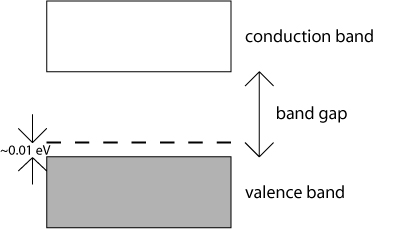
Doped semiconductors (either n-type or p-type) are known as extrinsic semiconductors. The activation energy for electrons to be donated by or accepted to impurity states is usually so low that at room temperature the concentration of majority charge carriers is similar to the concentration of impurities. It should be remembered that in an extrinsic semiconductor there is an contribution to the total number of charge carriers from intrinsic electrons and holes, but at room temperature this contribution is often very small in comparison with the number of charge carriers introduced by the controlled impurity doping of the semiconductor.
Direct and Indirect Band Gap Semiconductors
The band gap represents the minimum energy difference between the top of the valence band and the bottom of the conduction band, However, the top of the valence band and the bottom of the conduction band are not generally at the same value of the electron momentum. In a direct band gap semiconductor, the top of the valence band and the bottom of the conduction band occur at the same value of momentum, as in the schematic below.
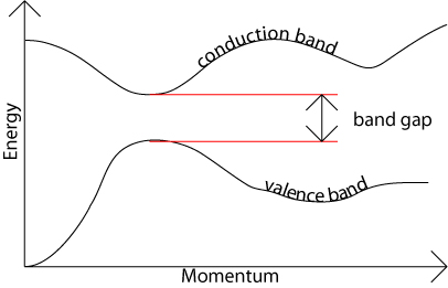
In an indirect band gap semiconductor, the maximum energy of the valence band occurs at a different value of momentum to the minimum in the conduction band energy:
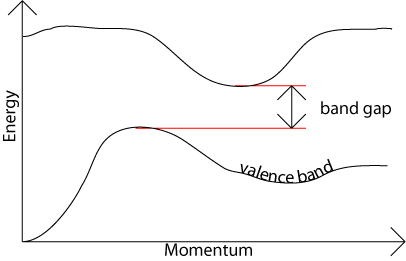
The difference between the two is most important in optical devices. As has been mentioned in the section charge carriers in semiconductors, a photon can provide the energy to produce an electron-hole pair.
Each photon of energy E has momentum p = E / c, where c is the velocity of light. An optical photon has an energy of the order of 10–19 J, and, since c = 3 × 10⁸ ms–1, a typical photon has a very small amount of momentum.
A photon of energy Eg, where Eg is the band gap energy, can produce an electron-hole pair in a direct band gap semiconductor quite easily, because the electron does not need to be given very much momentum. However, an electron must also undergo a significant change in its momentum for a photon of energy Eg to produce an electron-hole pair in an indirect band gap semiconductor. This is possible, but it requires such an electron to interact not only with the photon to gain energy, but also with a lattice vibration called a phonon in order to either gain or lose momentum.
The indirect process proceeds at a much slower rate, as it requires three entities to intersect in order to proceed: an electron, a photon and a phonon. This is analogous to chemical reactions, where, in a particular reaction step, a reaction between two molecules will proceed at a much greater rate than a process which involves three molecules.
The same principle applies to recombination of electrons and holes to produce photons. The recombination process is much more efficient for a direct band gap semiconductor than for an indirect band gap semiconductor, where the process must be mediated by a phonon.
As a result of such considerations, gallium arsenide and other direct band gap semiconductors are used to make optical devices such as LEDs and semiconductor lasers, whereas silicon, which is an indirect band gap semiconductor, is not. The table in the next section lists a number of different semiconducting compounds and their band gaps, and it also specifies whether their band gaps are direct or indirect.
Compound Semiconductors
In addition to group IV elements, compounds of group III and group V elements, and also compounds of group II and group VI elements are often semiconductors. The common feature to all of these is that they have an average of 4 valence electrons per atom.
One example of a compound semiconductor is gallium arsenide, GaAs. In a compound semiconductor like GaAs, doping can be accomplished by slightly varying the stoichiometry, i.e., the ratio of Ga atoms to As atoms. A slight increase in the proportion of As produces n-type doping, and a slight increase in the proportion of Ga produces p-type doping.
The table below list some semiconducting elements and compounds together with their bandgaps at 300 K.
|
Material |
Direct / Indirect Bandgap |
Band Gap Energy at 300 K (eV) |
|
|
|
|
| Groups III-V compounds |
GaAs |
Direct |
1.42 |
| Groups IV-IV compounds |
α-SiC |
Indirect |
2.99 |
| Groups II-VI compounds |
ZnO |
Direct |
3.35 |
Data from R.E. Hummel, Electronic Properties of Materials, 3rd edition, Appendix 4, p. 413.
Behaviour of the Fermi Energy
The Fermi-Dirac distribution was introduced in the section The Fermi-Dirac Distribution. The relevant equation to describe the distribution is
\[f\left( E \right) = \frac{1}{{\exp \left( {\left( {E - E_{\rm{F}} } \right)/{k_{\rm{B}}}T} \right) + 1}}\]
so that for a Fermi energy, \( E_{\rm{F}} \), of 5 eV, the distribution takes the form

as a function of temperature.
One feature that is very important about the Fermi-Dirac distribution is that it is symmetric about the Fermi energy. Hence for a simple intrinsic semiconductor, which has equal numbers of electrons in the conduction band and holes in the valence band, the Fermi energy must lie halfway between the valence band and the conductance band, regardless of the temperature, because each electron promoted to the conduction band leaves a hole in the valence band. This is shown in the band diagram below in which energy is plotted vertically against temperature horizontally.
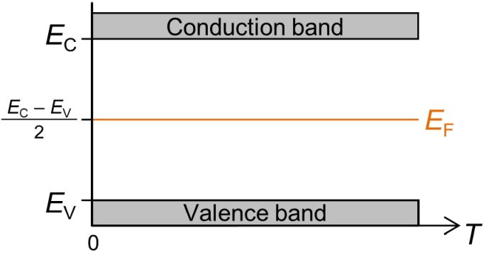
For an extrinsic semiconductor the situation is slightly more complicated. At absolute zero in an n-type semiconductor, the Fermi energy must lie in the centre of the gap between the donor level and the bottom of the conduction band. At low temperatures in such a semiconductor there are more conduction electrons than there are holes. If the donor level is more than half full, the Fermi energy must lie somewhere between the donor levels and the conduction band. At higher temperatures, when the donor level is completely depleted of electrons, and the contribution from intrinsic electrons to the overall electrical conductivity becomes more substantial, the Fermi energy tends towards that for an intrinsic semiconductor, i.e., halfway between the conduction and valence bands, and therefore in the middle of the band gap.
For p-type semiconductors the behaviour is similar, but the other way around, i.e., the Fermi energy starts midway between the valence band and the acceptor levels at absolute zero. It gradually increases as the temperature increases, so that at high temperatures it lies in the middle of the band gap as well.

Metal–Semiconductor Junction – Rectifying Contact
Before discussing the behaviour of a metal-semiconductor boundary, it is first necessary to introduce the concept of the work function. The work function of a material is the energy required to remove an electron from the level of the chemical potential (or Fermi energy) and give it enough energy to escape to infinity and arrive there with zero energy.
Albert Einstein first proposed the concept of the work function in his work on the photoelectric effect in metals. It was for this work, rather than for his work on relativity, that Einstein was awarded the Nobel prize in 1921.
When a metal and a semiconductor are joined, two possible types of contact can result, depending on the combination of metal and semiconductor used. The contact may be rectifying, which only allows current to pass in one direction. Alternatively, it could be ohmic, in which case current can pass in either direction. Here we will discuss the rectifying contact, sometimes called the Schottky barrier contact.
The schematic below shows a metal and an n-type semiconductor. The work functions of the metal and semiconductor have been labelled φm and φs respectively. The dashed line at the top represents the zero of energy at infinity. The energy difference labelled as \( \chi \) between the bottom of the conduction band and infinity is called the electron affinity of the semiconductor.
It should be noted that the above schematic is different to the illustrations showing energy bands plotted against momentum. Any horizontal change in a diagram such as that shown above represents a variation in the energy bands with position in real space.
In the metal the electron affinity is the energy which would be released if an electron were to fall in from infinity to the highest unoccupied energy level of the material. Hence, for a metal, the electron affinity is identical to the chemical potential or Fermi energy. This is also why the electron affinity for a semiconductor is the energy difference between the bottom of the conduction band and infinity.
The schematic above is an interactive animation. By clicking the button in the bottom right hand corner, the metal and the semiconductor are brought into contact. When contact is made, electrons can move between the metal and the semiconductor. The chemical potential (or Fermi energy) can be interpreted as the free energy per electron, so because φm > φs, the electrons in the conduction band of the n-type semiconductor can lower their energy by moving from the semiconductor into the metal.
Take a moment to navigate through the whole of the animation using the buttons at the bottom of the animation. As you read further through this section, keep returning to this animation as more is gradually explained.
The flow of electrons into the metal from the semiconductor on contact in this animation causes a slight negative charging of the metal, thereby repelling further flow of electrons from the conduction band of the semiconductor into the metal. The electric potential generated by the charging of the metal causes a deformation of the energy bands in the semiconductor close to the metal-semiconductor interface. The Fermi energy in the semiconductor also falls in this region, as higher energy electrons in the region adjacent to the metal have moved into the metal. The Fermi level of the metal is not appreciably affected because there are over 1010 times more valence electrons in the metal then there are conduction electrons in the semiconductor before contact – the addition of a few extra electrons from the semiconductor clearly makes little difference to the Fermi level in the metal.
Far from the metal-semiconductor interface, the band structure in the semiconductor is unaffected except for an overall displacement down in energy. The way to think about this change in the band structure is to consider the bands in the semiconductor to be 'pinned' at the interface with the metal. The Fermi energy in the region of semiconductor immediately adjacent to the metal moves in order to be in equilibrium with the metal. This has also to be true at distances in the semiconductor remote from the interface. At a large distance from the interface, the bands therefore have the same position relative to the shifted Fermi energy as they did before the metal and semiconductor were joined.
The most immediate consequence of making contact with the metal is that a region near to the metal-semiconductor interface is produced in the semiconductor which has no conduction electrons in it – this region is depleted of electrons in the conduction band. This region is therefore called the depletion layer, or the space charge region. This region is labelled in one of the intermediate steps of the illustration.
The depletion layer acts like an energy barrier. This barrier has a height of φm − χ for electrons moving from the metal to the semiconductor. The size of the barrier for electrons moving from the semiconductor to the metal is φm − φs, which is also equal to the total downward displacement of the bands in the semiconductor remote from the metal-semiconductor interface.
At a particular finite temperature, there will be electrons in the metal that can be thermally excited enough to overcome the energy barrier and diffuse into the semiconductor conduction band. Likewise, there will be electrons in the conduction band that will have enough thermal energy to diffuse from the semiconductor into the metal. In equilibrium these currents must be equal. If they were not, charging would occur at the interface and the band structure would be deformed until the diffusion currents of the electrons were identical in both directions. The higher energy barrier encountered in moving from the metal to the semiconductor is compensated for by the much larger numbers of free electrons in the metal.
In addition to the above diffusion current, there is also a drift current. The drift current is usually very small, and independent of the height of the energy barrier. It arises through the formation of electron-hole pairs in, or very near to, the depletion layer as a result of thermal excitation. The electron in such an electron-hole pair will be accelerated into the semiconductor (electrons 'roll' downhill), while the hole will be accelerated towards the boundary with the metal (holes 'float up' to the highest point). This contribution to the current is usually very small, and is dependent on the band gap of the semiconductor and the temperature. The total current across the junction is the net sum of the diffusion current and the drift current. At equilibrium, i.e. zero externally applied voltage, the net sum of these two currents is zero.
It should be noted that any hole created in the semiconductor near the metal, as a result of the thermal excitation of electrons into the conduction band, which then reaches the boundary with the metal successfully, will ultimately be destroyed by recombining with an electron from the metal.
If the metal is now connected to the negative terminal of a battery, and the semiconductor is connected to the positive terminal, there will be a greater negative charge on the metal, and the bands in the semiconductor will be further deformed.
This will increase the energy barrier and also the width of the depletion layer. This results in the diffusion current in both directions becoming negligible, because the energy barrier is large for both directions of diffusion. The contribution from the drift current will still remain, producing an extremely small and constant current of electrons from the metal into the positively biased semiconductor. This situation is called reverse bias.
When the metal is connected instead to the positive terminal of a battery, the negative charge on the metal is slightly reduced, and this will in turn reduce the deformation of the bands in the semiconductor. The resulting reduction in the width of the depletion layer, and the much lower energy barrier for electrons to move from the semiconductor into the metal results in a large net movement of electrons into the metal from the semiconductor, and therefore a net current flow. This is called forward bias.
If you have not already done so, take another look through the animation earlier in this section.
The overall current–voltage characteristic for a rectifying contact of this type is shown in the figure below. Note that the size of the current for reverse bias (negative voltage) has been greatly exaggerated.
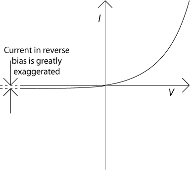
A similar rectifying device can also be made from the junction of a p-type semiconductor with a metal. In this case, φm has to be smaller than φs to form a rectifying contact. This can be represented schematically in a manner similar to that shown above for the n-type semiconductor–metal case. The animation below depicts the situation for a p-type semiconductor–metal rectifying contact.
The major difference here is that the sign of the voltage is reversed for a p-type device, i.e., it passes current when the metal is connected to the negative terminal, and blocks current when it is connected to the positive terminal.
Rectifying contacts can also be made from a junction between n-type and p-type semiconducting materials. Such a contact is termed a p–n junction and is discussed in the section of this TLP entitled The p–n Junction.
Metal–Semiconductor Junction – Ohmic Contact
When a metal and an n-type semiconductor are joined and φm < φs, electrons will flow from the Fermi energy level in the metal into the semiconductor conduction band to lower their energy. This will cause the Fermi energy of the semiconductor to move up into equilibrium with that of the metal. It will also deform the semiconductor bands, so that they curve upwards away from the metal. This situation is depicted in the animation below. Use the tabs to navigate through the animation.
This type of contact yields a linear relationship between the voltage applied and the current that flows across the junction. It is therefore called an Ohmic contact, because it obeys Ohm's law. This type of contact is also described as metallization, and is used to supply electric current into semiconductor devices.
The p–n Junction
As an alternative to the Schottky Barrier contact described in the section Metal–Semiconductor Junction - Rectifying Contact, a junction between an n-type semiconductor and a p-type semiconductor can be used as a rectifying contact. To see why, browse through the animation below. The various parts of the animation are discussed in detail later in this section, so do not be concerned if you do not understand every stage. You can return to this animation as you read more about the p-n junction.
It should be noted in the above animation that the relative quantity of electrons in the p-type material and the relative quantity of holes in the n-type semiconductor before they are joined together has been greatly exaggerated for the purposes of illustration. Both of these are minority carriers in their respective environments – remember that electrons are the majority carriers in n-type semiconductors and that holes are the majority carriers in p-type semiconductors.
When the two semiconductors are initially joined together, electrons will flow from the n-type semiconductor into the p-type semiconductor, and holes will flow from the p-type semiconductor into the n-type semiconductor. The Fermi energy levels of the two semiconductors will come to equilibrium, and the band structures will be deformed accordingly. A depletion layer is formed at the interface between the two types of doped semiconductor, in which numbers of electrons in the conduction band and holes in the valence band are both significantly reduced.
In equilibrium, there is an energy barrier for electrons to diffuse from the n-type semiconductor into the p-type semiconductor, and also for holes to move from the p-type semiconductor into the n-type semiconductor. These are the majority carriers. In addition, there will be currents from minority carriers, i.e., holes on the n-type side and electrons on the p-type side. For example, holes generated as a result of thermal excitation of electrons in the n-type semiconductor finding themselves in the depletion layer between the n- and p-type semiconductors will be swept over to the p-type side of the junction by the strong electric field within the depletion layer – since the electric field deters electrons from diffusing from the n-type side, it necessarily helps holes entering the depletion layer from the n-type side.
At equilibrium, the total current across the junction has be the same in both directions, so that the overall net current is zero. Any imbalance in current would mean that the system was not in equilibrium, and the bands would have to deform until the system returned to equilibrium.
If the n-type region is now connected to the positive terminal of a d.c. source and the p-type to the negative side, the bands will be further deformed at the interface, creating larger energy barriers for both electrons and holes to move across the junction and a wider depletion layer (i.e., a wider space charge region). In this situation of reverse bias, the only current is the very small contribution from the drift current arising from the minority carriers on both sides of the junction.
When the n-type region is connected to the negative terminal of a d.c. source and the p-type to the positive side, the depletion layer becomes narrower and the energy barriers are decreased in size. For this forward biasing, there will be a large net flow of electrons from the n-type semiconductor into the p-type semiconductor, and there will also be a net flow of holes moving into the n-type semiconductor from the p-type semiconductor.
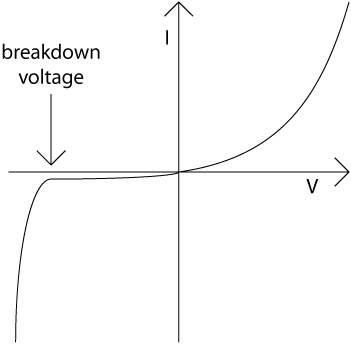
In a p-n junction rectifier, an increase in the strength of the reverse biasing will eventually lead to an increase in the current that flows. This is because for a sufficiently high field electric field, dielectric breakdown of the semiconductor occurs. The bias at which this occurs is called the breakdown voltage. The overall current–voltage characteristic of the p-n junction is shown in the diagram below.
Bipolar Transistor
Imagine two p-n junctions being joined back-to-back. This is the basic structure of the bipolar transistor. It is called bipolar because both electrons and holes carry current in the device. Bipolar transistors can occur in either n–p–n or p–n–p configurations. A schematic of a device in the n–p–n configuration is displayed below. Use the buttons to navigate through the animation.
There are three contacts to the transistor in the above animation. These are (i) the emitter, (ii) the base and and (iii) the collector. The emitter and the collector are n-type doped material, while the base is p-doped material. These are often labelled E, B and C.
With forward biasing applied to the emitter-base junction, and reverse biasing applied to the base-collector junction, the bands deform as shown in the animation. The energy barrier for an electron to diffuse from the emitter into the base is relatively low. Electrons injected from the emitter then diffuse through the thin base region before being accelerated through the strong reverse biased field between base and collector. Note that while the electrons are in the base region, they are minority carriers. The base has to be thin, so that electrons diffusing through are not lost by recombining with a hole, i.e., a majority carrier within the base region. Not only will electron current reduced when recombination occurs, but heat is also dissipated in this process, which is also undesirable.
Varying the base voltage changes the size of the energy barrier for electrons to be transferred from the emitter. In this way, the emitter-base voltage can be used to modulate the flow of current from emitter to collector. The applied voltage can also be used to completely stop the current flowing through the device, in effect using the transistor as a switch. It is this switching function which is used in logic circuits, such as those used in computers. A switch closed is a binary 0 (no current flow from emitter to collector), while a switch open is a binary 1 (current flow occurs between emitter and collector).
Metal Oxide Semiconductor Field Effect Transistor (MOSFET)
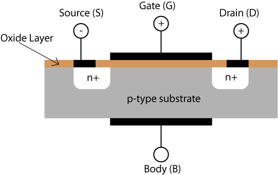
The metal oxide semiconductor field effect transistor (MOSFET) is one of the cornerstones of modern semiconductor technology. The general structure is a lightly doped p-type substrate, into which two regions, the source and the drain, both of heavily doped n-type semiconductor have been embedded.The symbol n+ is used to denote this heavy doping.
The source and the drain are about 1 μm apart. Metallized contacts are made to both source and drain, generally using aluminium. The rest of the substrate surface is covered with a thin oxide film, typically about 0.05 μm thick. The gate electrode is laid on top of the insulating oxide layer, and the body electrode in the above diagram provides a counter electrode to the Gate. The thin oxide film contains silicon dioxide (SiO2), but it may well also contain silicon nitride (Si3N4) and silicon oxynitride (Si2N2O).
The p-type doped substrate is only very lightly doped, and so it has a very high electrical resistance, and current cannot pass between the source and drain if there is zero voltage on the gate. Application of a positive potential to the gate electrode creates a strong electric field across the p-type material even for relatively small voltages, as the device thickness is very small and the field strength is given by the potential difference divided by the separation of the gate and body electrodes.
Since the gate electrode is positively charged, it will therefore repel the holes in the p-type region. For high enough electrical fields, the resulting deformation of the energy bands will cause the bands of the p-type region to curve up so much that electrons will begin to populate the conduction band. This is depicted in the animation below which shows a cross section through the region of the p-type material near the gate electrode. Click the button to increase the voltage applied to the gate electrode.
The population of the p-type substrate conduction bands in the region near to the oxide layer creates a conducting channel between the source and drain electrodes, permitting a current to pass through the device. The population of the conduction band begins above a critical voltage, VT, below which there is no conducting channel and no current flows. In this way the MOSFET may be used as a switch. Above the critical voltage, the gate voltage modulates the flow of current between source and drain, and may be used for signal amplification.
This is just one type of MOSFET, called 'normally -off' because it is only the application of a positive gate voltage above the critical voltage which allows it to pass current. Another type of MOSFET is the 'normally-on', which has a conductive channel of less heavily doped n-type material between the source and drain electrodes. This channel can be depleted of electrons by applying a negative voltage to the gate electrode. A large enough negative voltage will cause the channel to be closed off entirely.
'Normally-off' MOSFETs are used in a wide variety of integrated circuit applications. AND gates, NOT gates and NAND gates are all made from these type of MOSFETs and are essential components of memory devices.
Summary
The purpose of this teaching and learning package has been to give a very basic introduction to semiconductors.
By the end of this package you should be conversant with various aspects of terminology used to describe semiconducting materials, such as n-type semiconductor, p-type semiconductor, electrons, holes, band gap, majority carrier, minority carrier, work function, chemical potential, Fermi level, electron affinity, forward bias, reverse bias, Schottky barriers and Ohmic contacts. You should have an appreciation of what types of materials are semiconductors and what distinguishes wide-band-gap semiconductors from insulators. You should also be able to appreciate how very simple devices made from semiconducting materials such as p-n junctions and MOSFETs are able to respond to applied voltages.
Finally, the textbooks listed in the Going further section should be consulted for greater detail about the different topics covered in this TLP.
Questions
Quick questions
You should be able to answer these questions without too much difficulty after studying this TLP. If not, then you should go through it again!
-
What are the majority carriers of electric current in B-doped Si?
-
At absolute zero, which of these statements describes the position of the Fermi energy in an n-type semiconductor?
-
At room temperature, which of these statements describes the position of the Fermi energy in an n-type semiconductor?
-
Which of the following junctions is not rectifying?
-
The work function of gold is 4.8 eV and the electron affinity of silicon is 4.05 eV. Silicon has a band gap of 1.12 eV at 300 K. What is the barrier height at 300 K preventing the majority carriers in n-type silicon from crossing between a piece of n-type silicon and gold where the Fermi energy of the n-type silicon is 0.25 eV below the bottom of the conduction band?
Going further
Books
There are many excellent textbooks which give an introduction to semiconductors. The following textbooks are just a few examples:
- Solid State Physics, N.W. Ashcroft and N. D. Mermin. (Harcourt Brace 1976)
- Solid State Physics, J.S. Blakemore (Saunders 1974)
- The Electronic Structure and Chemistry of Solids, P.A. Cox (Oxford, 1987)
- Electronic Properties of Materials, R.E. Hummel (Springer-Verlag 2001)
- Principles of Electronic Materials and Devices, S.O. Kasap (McGraw-Hill 2006)
- Introduction to Solid State Physics, C. Kittel (Wiley 1996)
- Electronic Materials Science, J.W. Mayer and S.S. Lau (Macmillan 1990)
- Introductory Semiconductor Device Physics, G. Parker (Institute of Physics 2004)
- The Solid State, H.M. Rosenberg (OUP 1988)
- Lectures on the Electrical Properties of Materials, L. Solymar and D. Walsh (OUP 1993)
- Solid State Electronic Devices, B.G. Streetman and S.K. Banerjee (Pearson Prentice Hall 2006)
Some of these texts are deliberately written as introductory texts for undergraduates
in physics, chemistry, materials science and electrical engineering, while others
are meant for graduate students in these areas and lead the reader into research-level
material.
Websites
There are now a great many web sites containing material relevant to this TLP. These web sites offer various levels of sophistication in their treatment of semiconductors. Examples are:
- http://nobelprize.org/educational_games/physics/semiconductors/
- http://nobelprize.org/educational_games/physics/transistor/function/index.html
- http://nobelprize.org/educational_games/physics/integrated_circuit/history/index.html
These three Nobel Prize sites are aimed at the general public and give fairly simple, but useful, treatments.
- http://en.wikipedia.org/wiki/Semiconductor
The Wikipedia source article is a gateway to further articles on semiconductors
Academic consultant: Kevin Knowles (University of Cambridge)
Content development: Chris Dunleavy and David Brook
Web development: David Brook and Lianne Sallows
This DoITPoMS TLP wass funded by the UK Centre for Materials Education and the Department of Materials Science and Metallurgy, University of Cambridge.
Additional support for the development of this TLP came from the Worshipful Company of Armourers and Brasiers'

