Flux divergence (II)
Variations in Material
Different materials are used within an integrated circuit: for example, the Si substrate, W vias and Al interconnects. Differences in diffusion rates between two materials result in atomic flux divergence at the interface between them.
If the current flows from a material with a higher diffusivity to one with a lower diffusivity, the interface between the materials is a region of mass accumulation. Conversely when current flows from material with a lower diffusivity to another material with a higher diffusivity, void formation takes place at the interface. Electromigration-induced damage is most evident where the change in diffusivity is very large, e.g. at a Cu/barrier interface or an Al line/ W via interface.
Two main examples of this can be seen in: contacts and vias.
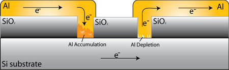
- Contacts
When current flows through the contacts, electromigration causes metal atoms to move away from and towards the semiconductor interface. The inability to replenish metal that has been removed from and the inability to remove metal brought to the semiconductor interface results in a region of mass divergence. At the contact window either accumulation or depletion of Al occurs, depending on the direction of current flow.
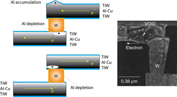
- Vias
The IC architecture requires use of successive interconnect levels and therefore of vias that enable current to flow between the layers. For Al-based metallization, W plug vias are commonly employed due to their high reliability, though structures consisting of Al-Cu vias can be used but are more difficult to make. As Al metallization tends to migrate whilst W exhibits negligible atomic transport (as shown in values of self-diffusion below), via-interconnect interfaces become sites of potentially large mass divergences.
The bulk lattice diffusivity values of Al and W at 300 K (assumed service temperature of the IC) are*:
DAl, bulk = 3.2×10⁻²⁹ m2 s-1
0 < DW, bulk < 5×10-88 m2 s-1 (negligible)
*Values calculated from data in Smithells Metals Reference Book, 6th Ed., Mechanisms of Diffusion p.13-11; E.A. Brandes (editor), Butterworths, London (UK), 1983.
Source of SEM image of void formation at a via; R. Rosenberg et. al.: Copper metallization for high performance silicon technology, Annu. Rev. Mater. Sci. 20 p.229, 2000.
Degradation at vias is dependent not only on composition and grain structure, but also on the direction of current flow. The two modes of electromigration damage are shown above (in a schematic form and from an SEM micrograph). Voids form where the electrons flow away from the via, while a hillock forms when electrons flow towards the via.
In addition, thinned metal conductors and corners induce excessive Joule-heating effects and current crowding that lead to accelerated degradation.
![]()
Variations in Temperature
Temperature differences along the metallization line cause flux divergence because the diffusion coefficient is dependent on temperature. At higher temperatures, diffusion rates are increased. If there is a variation of temperature along the metal line, regions of accumulation and void growth would develop over time. Although the silicon substrate acts as a very good heat sink, the temperature along a line can vary because of heat generation in the underlying semiconductor components and because of local heating due to current crowding in the metallization itself.