Electromigration (all content)
Note: DoITPoMS Teaching and Learning Packages are intended to be used interactively at a computer! This print-friendly version of the TLP is provided for convenience, but does not display all the content of the TLP. For example, any video clips and answers to questions are missing. The formatting (page breaks, etc) of the printed version is unpredictable and highly dependent on your browser.
Contents
Main pages
Additional pages
Aims
On completion of this TLP package, you should:
- understand the process of electromigration
- be aware of how damage is caused by electromigration and the ways in which such damage is minimized
- know the reasons for changing from Al-based to Cu-based metallization.
Before you start
-
It would help to look through the Diffusion TLP, but this TLP is mostly self-explanatory.
Introduction
The use of microelectronic devices within our daily lives has increased vastly resulting in the transformation of our lives by recent scientific and technological advances. Electromigration is a principal wear-out mechanism of integrated circuits (IC), thus limiting their reliability. Reliability is important for the success in the microelectronics industry as a product is expected to work for an extended period of time without failure. This makes electromigration an area of intense research as more and more is demanded from microprocessors – to be faster, with smaller components and cheaper.
![]()
History
An IC contains various interconnected semiconductor components, such as transistors, resistors, capacitors and diodes. The first integrated chip contained tens of transistors within a chip area of 1 cm2, and can now be called “Small-Scale Integration” (SSI). To find out more about the different parts of an integrated circuit, click here.
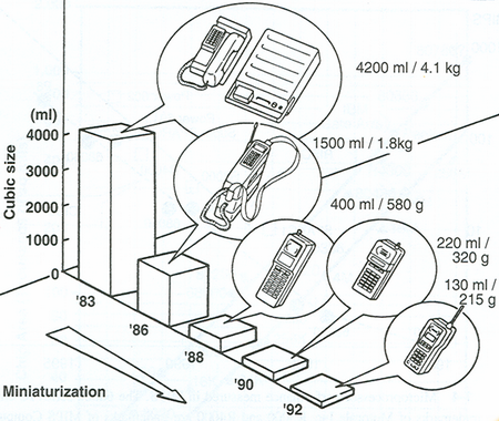
With time, there has been a reduction of the dimensions of personal computing systems, from the size of a desktop, to a notebook, to a palmtop, to a credit card, to a watch, eventually to the size of a finger ring!
Concurrently, there has been a change in volume and complexity of wireless communication system.
Reprinted from ‘Reliability and Failure of Electronic Materials and Devices’ by Milton Ohring, Copyright 1998, with permission from Elsevier.
Currently, a chip area of 1 cm2 or smaller contains hundreds of thousands of transistors to several million – “Very Large-Scale Integration” (VLSI) – making it possible to fabricate a Central Processing Unit (CPU) on a single integrated circuit. The industry now uses the terminology of “Ultra-Large-Scale Integration” (ULSI), for chips containing more than a million transistors and to emphasize chip complexity.
This continuous stream of achieving higher levels of integration brings about an exponential growth in the power of computing and communications technology to consumers and businesses worldwide. This is described by Moore’s Law.
Moore’s Law states that:
The number of transistors on an integrated circuit doubles about every two years.
Today, adding transistors in pace with Moore’s Law continues to drive increased functionality, performance and decreased cost of computing and communications technology. The price of an individual transistor has decreased drastically from $45 (in the 1950s) to less than a hundred-thousandth of a cent (currently - 2005)!
Click this link to view a graph depicting the rapid growth in the number of transistors integrated onto a single chip.
The dramatic miniaturization has involved not only the semiconductor components of an IC but also the conducting lines linking them (the interconnects – part of the metallization on a device). Changes relevant for electromigration-induced failure of interconnects include:
- line widths shrinking from 10 mm to 0.19 μm, which will become even finer in the future.
- total length of interconnect lines on a single IC increasing from several cm to several km (reaching lengths of about 5 km).
- current densities increasing from 108 A m–2 to 1010 A m–2.
- number of metal levels increasing from 1 to 7 – this is because the number of components has increased so vastly that a single level on the top of the silicon substrate is insufficient to interconnect all the semiconductor components in the substrate, thus requiring multiple levels of metallization lines.
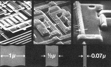
Line widths decreasing from 1 μm to 0.5 μm (for research purposes line widths as small as 0.07 μm have been used).
Reprinted from ‘Reliability and Failure of Electronic Materials and Devices’ by Milton Ohring, Copyright 1998, with permission from Elsevier.
These changes all increase the likelihood of electromigration-induced failure of the metallization and they drive further research to reduce the effect of electromigration. The latest development is the move away from aluminium-based to copper-based metallization lines.
The theory of electromigration
Electromigration is the transport of material in a conductor under the influence of an applied electric field. All conductors are susceptible to electromigration, therefore it is important to consider the effects the electrical current resulting from the applied field may have on the conductor.
The net force exerted on a single metal ion in a conductor has two opposing contributions: a direct force and wind force.
![]()
Direct Force
Application of an electric field results in an electrostatic pull being exerted on the metal ion core. The direction and magnitude of the electrostatic pull depend on the charge on the ion core, modified by screening effects. Positively charged ion cores (cations) are pulled towards the cathode, whilst negatively charged ion cores (anions) are pulled towards the anode. The direct force, Fd, is given by:
Fd = a Z e E = a Z e j ρ
where a = factor accounting for screening (a<<1); Z = actual valence of the atom; e = electron charge (1.6 x 10⁻¹⁹ C); j = current density (A m-2); ρ = resistivity (Ω m).
When electromigration in conductors was discovered, it was thought that the migration effects would be analogous to those in liquid electrolysis.
Consider for example, the electrolysis of the molten salt, NaCl. The Na+ ions move towards the cathode, whilst the Cl– ions move towards the anode (as shown in the diagram below), as the electric field is applied.
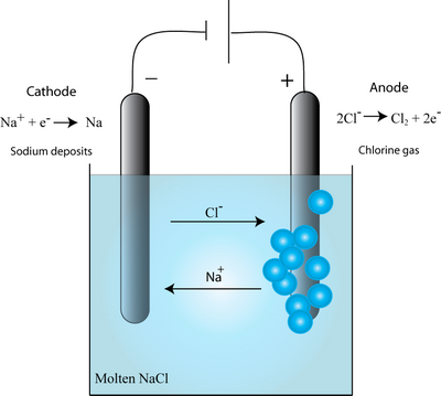
It was thought that the metal ions within a wire would always move towards the cathode as in electrolysis. While this is found in some cases, in the metallization of interest for ICs (which are based on good metal conductors) the migration was observed to be in the opposite direction – towards the anode. This startling effect results from the wind force.
![]()
Wind Force
Electrons move along the metallization line, carrying the current. These electrons tend to scatter. Electron scattering takes place at imperfections within the lattice: vacancies, impurities, grain boundaries, dislocations and even phonon vibrations of the metal ions from their ideal positions! The scattering of electrons gives us electrical resistance but it also results in a force exerted on the metal ion core.
An electron changes direction as a result of a scattering event. This change in direction is accompanied by an acceleration, which results in a force. The electrons are also accelerated within the electric field. When the overall electron drift velocity is established, the force on the ions due to electron scattering is in the direction of the electron flow – this is known as the wind force, Fw, which can be described as:
Fw = –eneλσiE
where ne = density of electrons;σi = cross-section for collision; λ = mean free path.
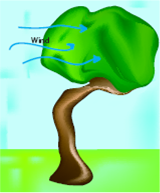
The term electron wind comes from an analogy with, for example, a tree being blown in the wind. The wind is analogous to the electron current, the leaves on the tree to the metal ions in a conductor.
![]()
Net Force
In good conductors, such as the ones used in IC metallization, the electron wind force is the dominant force felt by the ion cores, resulting in atomic migration towards the anode. The net force on the ions can be represented as:
Fnet = Fwind +Fdirect = ( Zw + Zd ) ejρ = Z*ejρ
where Zwind, Zdirect and Z* respectively refer to the effective valences for the wind force, direct force and the net force.
![]()
Diffusion
The migration of the metal ion cores occurs by diffusive jumps. In the cases of interest in metallization, this is self-diffusion or substitutional diffusion by the vacancy mechanism.
The rate of diffusion is described by the diffusion coefficient (or diffusivity) with units of m2 s–1. The diffusivity, D, has an Arrhenius dependence on temperature according to:
D = D0 exp (–Q/RT)
where D0 = constant (m2 s–1); Q = activation energy for diffusion (J mol–1); R = gas constant (8.314 J mol–1 K–1); T = absolute temperature (K).
The diffusion coefficient and the activation energy are dependent on the nature of the material.
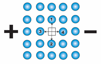
We depict above a 2-D section through a simple cubic metallic lattice showing a single vacant site. The vacancy can jump into either position 1, 2, 3 or 4 (i.e. it can exchange position with the atom in position 1, 2, 3 or 4). Without any external influence, the probability of the vacancy jumping into each site is equal, as its energy on every site is the same and the activation energy for a jump from site to site is always the same.
When an electric field is applied, the activation energies for a jump into sites 1 and 2 remain identical, whereas the activation energy for a jump into site 4 is smaller than that into site 3. This results in a biasing of vacancy diffusion jumps towards the cathode. This net flux of vacancies towards the cathode corresponds to the net flux of atoms (or ions) towards the anode. This flux of metal ions can be considered to be due to the effective charge, Z*, on the ion and the associated net force as described above.
J = CDFnet/RT = CDZ*eρj/RT
where J = atomic flux (atoms m2 s–1) ; C = atomic concentration (atoms m–3); D = diffusivity (m2 s–1).
Note that this overall net flux is exceedingly minute. There is only a very slight biasing of atomic movement e.g. in 1000 atoms 499 would diffuse towards the anode whilst 501 diffuse towards the cathode, resulting in a net of 2 atoms migrating towards the cathode. Electromigration is a very slow process, taking time.
Electromigration damage
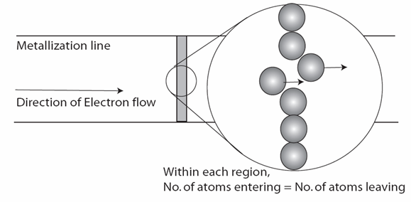
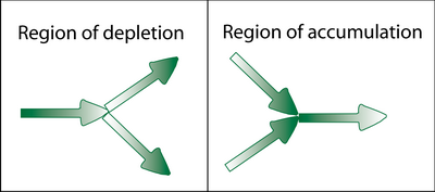
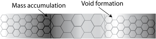
Electromigration is the mass transport in a metallic conductor due to the momentum transfer between conducting electrons and diffusing metal atoms. Uniform electromigration within the metallization lines, if it could be maintained, would not be damaging: in steady-state, no damage should be observed other than at the beginning and end of the metallization line. This is because along the metallization line the number of atoms arriving in a given local volume is equal to the number of atoms leaving the volume, as shown in the diagram below.
Damage to the metallization lines is caused by divergences in atomic flux. When the amounts of matter leaving and entering a given volume are unequal, the associated accumulation or loss of material results in damage.
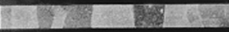
When atomic flux into a region is greater than the flux leaving it, the matter accumulates in the form of a hillock or a whisker. If the flux leaving the region is greater than the flux entering, the depletion of matter ultimately leads to a void. These features are shown in the SEM micrographs below.
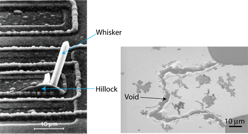
Source of images: (left) Microelectronic Materials by CRM Grovenor, IOP Publishing Ltd, Bristol (UK); (right) Dr Lo Veng Cheong
Regions of void formation are usually associated with neighbouring regions of material accumulation, as atoms are transported from one region to the other. Stresses develop within the metallization line as a result of the mass transport.
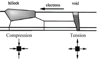
Source of image: O. Kraft, J.E. Sanchez Jr., M. Bauer, E. Arzt: Quantitative analysis of electromigration damage in Al-based conductor lines. J. Mat. Res. 12 (1997) p.2027-2037.
A stress gradient builds up within the metallic line and opposes the electromigration force. The formation of voids and hillocks partially relieves these stresses. A void forms to relieve tensile stresses, whilst hillock growth relieves compressive stresses.
The growth of voids and hillocks can be viewed in the videos below:
DoITPoMS standard terms of use
Video showing hillock growth (wide metallization lines)
Video showing void growth and migration (wide metallization lines)
Video showing void growth (modern, narrow metallization lines)
Voids and hillocks are detrimental to the metallization lines because a growing hillock could come into contact with other metallization lines resulting in a short circuit, an unintended pathway for the electricity to flow. As a void grows, the effective cross-sectional area of the metallization line decreases. This results in both an increase in resistance and current density within the system. The void ultimately leads to an open circuit when no material bridges across it.
These effects disrupt the intended functioning of the integrated circuit and result in failure. The nature of a microprocessor chip makes repair impossible and the failed chip has to be replaced.
Flux divergence (I)
Divergences in atomic flux, J, within the metallization line result in damage. The origins of non-steady-state mass transport (i.e. transport such that the concentration of atoms, C changes locally) can be understood in terms of the equation of continuity; for example, in one dimension:
\[\frac{{\partial C}}{{\partial t}} = - {\left. {\frac{\partial }{{\partial x}}\left\{ {\frac{{CDZ*e\rho j}}{{RT}}} \right\}} \right|_{T = {\rm{constant}}}} - {\left. {\frac{\partial }{{\partial T}}\left\{ {\frac{{CDZ*e\rho j}}{{RT}}} \right\}} \right|_{x = {\rm{constant}}}}\frac{{\partial T}}{{\partial x}}\]
| from local structural property gradients at constant T | from T gradients and thermally dependent properties |
Therefore when:
∂C/∂t < 0: mass depletion occurs and voids form (positive flux divergence)
∂C/∂t > 0: mass accumulates in growths – hillocks and whiskers (negative flux divergence)
∂C/∂t = 0: there is no change in atomic concentration and no damage occurs.
All the metal parts through which current flows in integrated circuits are potentially susceptible to electromigration effects. Different aspects are important in interconnects, contacts and vias.
As an added complication, the system observed is never static. Interactions within the metallization line result in the:
- movement of grain boundaries (grain growth)
- induction of heating
- recrystallization of the grain structure
- subtle evolution of microstructure and chemical composition.
The main contributions to flux divergence within metallization lines are: variations in microstructure, material or temperature.
![]()
Variation in Microstructure
Grain boundaries within Al-based metallization lines act as fast diffusion paths compared to the bulk system. The atomic environment at a boundary is less confining and contains fewer obstacles to diffusion. Accordingly, the activation energy for grain boundary diffusion is lower than that for bulk diffusion. As diffusion at grain boundaries far exceeds transport through the bulk of grains, the overall rate of atomic transport is greatly affected by the grain size, which determines the area of grain boundary in a given volume of sample.
The grain structure within metallization lines can vary from place to place: for example, the deposition technique would affect the degree of variation of microstructure. The associated property variations also lead to electromigration damage. Differences in microstructure or properties can be very large or barely perceptible, involving variations in grain orientation, grain size, chemical composition, atomic diffusivity, effective valency and vacancy generation within the grain structure.
Electromigration-induced damage is profoundly affected by grain structure: for example single-crystal aluminium stripes exhibit “infinite” life. This is because atomic diffusion and drift, for a metallization based on Al, are dominated by transport along grain boundaries rather than transport through the bulk of grains.
Some examples of microstructural variations are:-
A film with a uniform grain size has a network of grain boundaries meeting at triple points (strictly, triple lines in 3-D). In annealed thin films it is usual for the grain structure to be in a 2-D pattern, with each grain occupying the full thickness of the film.

For a common metallization, such as Al-Cu, where the migrating atoms are solely confined to grain boundaries, it is possible to get divergences in mass transport at the triple points found in interconnect and contact lines. The atomic diffusivity in a given boundary can vary widely, depending on the structure of the boundary, which is related to the crystallographic misorientation of the grains. But even if we assume that all the grain boundaries are high-angle boundaries with similar diffusivities, it can easily be understood that flux divergences must arise at triple points.
When the direction of migration is such that one grain boundary leads into and two boundaries lead away from a triple point, the negative flux divergence can lead to the formation of a void. The converse is true when two boundaries lead into a triple point and one leaves, giving mass accumulation and possible hillock formation.
It would be assumed that a metallization line consisting of numerous triple points would be full of defects. This is not the case, as described by the concept known as the Blech length. Often, no damage is observed at triple points because they are closer than this critical length for damage e.g. for a current density of 1 x 10⁹ A m2, a line length of several hundred micrometers will not be susceptible to electromigration. A longer metallization line would have a larger number of triple points and hence an increased likelihood of this kind of failure. However, other factors come into effect as metallization line length increases, thus resulting in yet further damage.
A fine-grained region contains more grain boundaries for atomic migration, than a coarse-grained region. Accumulation of atoms therefore occurs when atomic migration is from a fine-grained region moving into a coarser grained region. Conversely, voiding occurs when the migration is from a coarse to a finer grain size.
To avoid damage-inducing mass divergences, a bamboo-like grain structure (as shown in the SEM micrograph below) is desirable. The lack of continuous grain boundary paths for diffusion results in negligible mass transport along grain boundaries. The driving force for electromigration is predominantly perpendicular to the grain boundaries.
SEM micrograph of a metallization line containing a bamboo structure - grain boundaries are perpendicular to electron flow. (Reprinted with permission from: A.G. Domenicucci et.al: Effect of copper on the microstructure and electromigration lifetime Ti-AlCu-Ti fine lines in the presence of tungsten diffusion barriers. J. Appl. Phys. 80, p4952. Copyright 1998. American Institute of Physics.)
The animation below shows bamboo structure and its resistance to EM-damage.
Flux divergence (II)
Variations in Material
Different materials are used within an integrated circuit: for example, the Si substrate, W vias and Al interconnects. Differences in diffusion rates between two materials result in atomic flux divergence at the interface between them.
If the current flows from a material with a higher diffusivity to one with a lower diffusivity, the interface between the materials is a region of mass accumulation. Conversely when current flows from material with a lower diffusivity to another material with a higher diffusivity, void formation takes place at the interface. Electromigration-induced damage is most evident where the change in diffusivity is very large, e.g. at a Cu/barrier interface or an Al line/ W via interface.
Two main examples of this can be seen in: contacts and vias.
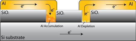
- Contacts
When current flows through the contacts, electromigration causes metal atoms to move away from and towards the semiconductor interface. The inability to replenish metal that has been removed from and the inability to remove metal brought to the semiconductor interface results in a region of mass divergence. At the contact window either accumulation or depletion of Al occurs, depending on the direction of current flow.
- Vias
The IC architecture requires use of successive interconnect levels and therefore of vias that enable current to flow between the layers. For Al-based metallization, W plug vias are commonly employed due to their high reliability, though structures consisting of Al-Cu vias can be used but are more difficult to make. As Al metallization tends to migrate whilst W exhibits negligible atomic transport (as shown in values of self-diffusion below), via-interconnect interfaces become sites of potentially large mass divergences.
The bulk lattice diffusivity values of Al and W at 300 K (assumed service temperature of the IC) are*:
DAl, bulk = 3.2×10⁻²⁹ m2 s-1
0 < DW, bulk < 5×10-88 m2 s-1 (negligible)
*Values calculated from data in Smithells Metals Reference Book, 6th Ed., Mechanisms of Diffusion p.13-11; E.A. Brandes (editor), Butterworths, London (UK), 1983.
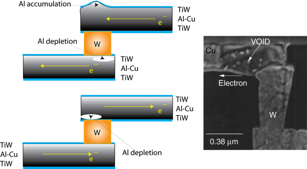
Source of SEM image of void formation at a via; R. Rosenberg et. al.: Copper metallization for high performance silicon technology, Annu. Rev. Mater. Sci. 20 p.229, 2000.
Degradation at vias is dependent not only on composition and grain structure, but also on the direction of current flow. The two modes of electromigration damage are shown above (in a schematic form and from an SEM micrograph). Voids form where the electrons flow away from the via, while a hillock forms when electrons flow towards the via.
In addition, thinned metal conductors and corners induce excessive Joule-heating effects and current crowding that lead to accelerated degradation.
![]()
Variations in Temperature
Temperature differences along the metallization line cause flux divergence because the diffusion coefficient is dependent on temperature. At higher temperatures, diffusion rates are increased. If there is a variation of temperature along the metal line, regions of accumulation and void growth would develop over time. Although the silicon substrate acts as a very good heat sink, the temperature along a line can vary because of heat generation in the underlying semiconductor components and because of local heating due to current crowding in the metallization itself.
Avoiding electromigration problems
At the time of publication of this TLP, in the International Technology Roadmap for Semiconductors, the top three challenges facing the industry were given as:
- Problems with integration and material characterization arising from rapid introduction of new materials and processes, which are necessary to meet conductivity requirements and reduce dielectric permittivity.
- Engineering interconnect structures which can be manufactured and are compatible with new materials, because there is a lack of interconnect/packaging architecture design optimization tools to include: integration complexity, chemical mechanical polishing (CMP) damage, resist poisoning, and dielectric constant degradation.
- Achieving necessary reliability by using new materials, structures and processes; and the need for detection, testing, modelling and control of failure mechanisms.
Failure mechanisms, such as electromigration, create reliability problems. Therefore, the need for reliability within ICs drives research to make further development in avoiding electromigration failure. This is a huge challenge to the microelectronics industry as everything tends towards smaller and smaller components.
There are several factors affecting the lifespan of interconnects. These can be divided into two classifications: material and processing; and external conditions.
Material and Processing |
External Conditions |
|
|
Electromigration failures take time to develop and the early stages are difficult to detect. As electromigration damage is cumulative, it is best to prevent damage from occurring during the lifetime of the device.
Careful design helps to prevent electromigration-induced damage. This includes: ensuring that current densities in all parts of the circuit are limited, so as to have sufficient current to run the device yet minimizing any potential electromigration damage; choosing metallization compositions to limit electromigration degradation; and making good selections for passivating thin films placed over metal lines to prevent extrusions caused by electromigration. An example of this is the move towards changing Al-based metallization to Cu-based metallization.
Grain structure of metallization lines can also be optimized (see Flux Divergence - Differences in Grain Size)
When designing a device, the median lifetime is often estimated using Black’s Law:
\[{t_{50}} = c{j^{ - n}}{e^{\frac{{{E_e}}}{{kT}}}}\]
where t50 = median time to failure of metal lines subjected to electromigration (hrs); c = constant based on the metal line properties (units depend on exponent n); j = current density (A m-2); n = value between 1 and 7 (though commonly 2); Ee = activation energy (J) [within the range 0.5–0.7 for Al]; k = Boltzmann constant (1.38×10⁻²³ J K-1); and T = temperature (K).
Black’s law is an empirically found relationship. This relationship is found by performing experiments at higher current densities and temperatures, to speed up the time to failure. The data is then extrapolated down to the service conditions for the current density and temperature of the IC.
Optimising the median lifetime is difficult, as exact and verified values are required for the current densities in order to make a reasonable estimation. It is challenging to obtain the data required. It is also uncertain if such an extrapolation of data is possible for a suitable estimation. Therefore, it is often that an attempt can only be made to limit the current density, in order to give the desired lifetime.
An alternative is to make use of other materials and their properties. Currently, refractory or barrier layers e.g. TiN, TiW, Cr2O3 are used to carry the current after an open circuit results from void formation, thus giving the device a longer lifetime before failure.
Alternatives to aluminium metallization
Technological pressures on the speed and reliability of integrated circuits has caused a need for changes to be made in the choices of materials used for metallization lines today. In selecting a material for metallization, it is necessary to consider what its desirable properties would be. These include:
- low resistivity
- mechanical stability, good adherence, and low stress
- easy to form
- easy to etch for pattern generation
- stable throughout processing, including: high temperature sinter, dry or wet oxidation, gettering, phosphorus glass (or any other materials) passivation, and metallization
- should not contaminate devices, wafers or working apparatus
- should be stable in oxidation ambients and is able to form a stable oxide
- no reaction with other components
- good surface smoothness
- low contact resistance, minimal junction penetration and low electromigration for use in window contacts
- very low cost
During the growth of the microelectronics industry, metallization lines have moved from the use of pure Al to Al-Cu alloy and currently to pure Cu.
![]()
Using Pure Aluminium
Commercially, it would be assumed that a material having the lowest resistivity would be used for IC interconnections. This is because, the lower the resistivity of the material, the smaller the resultant RC-delay, and the faster the signal transmission between devices – in order to be useful, resistivities must be below 50 μΩ cm.
Metal |
Electrical resistivity (at 20 ºC) / µΩ cm |
Al |
2.65 |
Data obtained from Metals Handbook, 8th Edition, ASM, Metals Park, Ohio.
Yet, the standard interconnection material previously used was Al, despite having other materials such as Ag, Cu and Au with lower resistivity values (as shown in the table). This is because it was found that:
- Ag is too prone to attack by S and O, and could not maintain its low resistivity over the device lifetime.
- Cu is prone to oxidation resulting in a vast increase in resistivity of the material.
- Ag and Au are very difficult to deposit as very low resistance films.
Al has low resistivity and can be easily deposited. It can be dry etched, does not contaminate Si as it forms a protective Al2O3 oxide layer which prevents further oxidation, has excellent adhesion to dielectrics, and is able to form ohmic contacts.
These factors resulted in the universal use of Al-based metallization in ICs. Unfortunately, Al has a problem forming contacts with shallow junctions, has difficulty achieving a good mechanical and electrical connection as a vacuum deposited thin film and is very prone to electromigration failure.
![]()
Using Aluminium-Copper Alloys
Due to problems associated with electromigration in pure Al metallization, there was a real need to improve the metallization. In the mid 1960s, a mis-focused electron beam evaporated some Cu, instead of the charge metal (Al). The resultant Al-Cu alloy films were found to be significantly resistant to electromigration.
This is shown in the table below, as the amount of Cu content increases the critical product (jl)c is increased and the effective charge, Z*, is decreased.
|
Cu content (wt%) |
Critical product (jl)c/ A cm-1 |
Effective charge number, Z* |
Al standard |
0 |
244 |
18 |
Data from: ‘Quantitative analysis of electromigration damage in Al-based conductor lines’ by O. Kraft et.al. J. Mater. Res., 12 (1997) 2027.
Reducing the effect of electromigration
A commonly used Al-Cu alloy is Al-1.5at%Si-4at%Cu. Despite its increase in resistivity from 2.86 μΩ cm (pure Al) to 3 μΩ (Al-Cu alloy), the improvement of electromigration resistance made Al-Cu alloys the system of choice in metallization.
There are several reasons for the increase in electromigration resistance:
- As most mass transport in Al occurs along grain boundaries, the addition of Si and Cu reduced the grain boundary diffusion rate, by increasing the activation energy of grain-boundary diffusion.
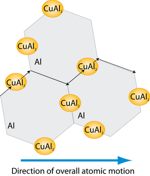
- The addition of Cu to the Al alloy, results in the formation of CuAl2 precipitates. These precipitates form primarily on grain boundaries, impeding grain boundary diffusion. The precipitates also act as reservoirs of Cu, delaying any damage, as the precipitate must dissolve before the level of Cu in grain boundaries can fall significantly. Dissolution is rather slow as a steady-state flow of Cu can be established from precipitate to precipitate before migration takes place.

Using Pure Copper
The trend towards narrower interconnections, and faster and more reliable devices resulted in the examination of the possibility of using Cu-based metallization. It was found that the change to a Cu-based material greatly improved the reliability of devices.
A comparison (see table below) shows the reasons for the currently increasing use of Cu-based metallization in the microelectronics industry:
Advantages of Cu |
Disadvantages of Cu |
|
|
Due to the favourable properties of Cu, it is possible for the chip size to be reduced, whilst increasing the speed and complexity of the device.
Cu has proved to be an excellent metallization material as it has an improved current carrying capability and high electromigration resistance. The disadvantages have been overcome using new thin-film technology and careful materials selection. It is therefore possible for component size to be further reduced, increasing the speed and complexity of the device.
This is sufficient for now, though there is a continuing need to achieve high conductivity and minuscule dielectric constants for future devices. Therefore, in order for the microelectronics industry to keep up with Moore’s Law and the ever increasing consumer needs, there needs to be introduction of new materials and processes.
Summary
This TLP has covered several points:-
- The reliability of microelectronic devices is important, as our lifestyles depend on the current technology and we expect continuing improvements in performance. Electromigration reduces device reliability, which is a problem for the electronic industry.
- Electromigration is the transport of material in a conductor under the influence of an applied electric field.
- Electromigration phenomena occur in all conductors on application of an electric field. Damage is commonly observed within narrow metallization lines in integrated circuits, as they are exposed to particularly high current densities.
- The electromigration force, which causes atomic migration, is a combination of two forces – the direct force and the wind force, related by:
Fnet = Fwind + Fdirect = Z*ejρ
where Z* = effective charge; j = current density (A m-2); and ρ = resistivity (Ω m).
Mass atomic transport towards the cathode occurs as the net force biases the net diffusion direction.
- Damage induced by electromigration results in hillock and void formation. Electromigration-induced damage is caused by divergences in atomic flux, themselves caused by place-to-place variation in:
- Microstructure
- Material
- Temperature
- Choosing the best materials for use in an integrated circuit, the most suitable processing methods and good device design can assist in reducing the resultant electromigration damage.
- The device lifetime can be roughly estimated using Black’s Law to extrapolate median time to failure at service temperature from accelerated test conditions:
\[{t_{50}} = c{j^{ - n}}{e^{\frac{{{E_e}}}{{kT}}}}\]
where t50 = median time to failure of metal lines subjected to electromigration (hrs); c = constant based on the metal line properties (units depend on exponent n); j = current density (A m-2); n = value between 1 and 7 (though commonly 2); Ea = activation energy (J) [within the range 0.5–0.7 for Al]; k = Boltzmann constant (1.38×10⁻²³ J K-1); and T = temperature (K).
- Due to the increased miniaturization of microelectronic devices, there is a need for new materials and processes to be used for metallization lines. One such development is the change from Al-based to Cu-based metallization in high performance devices. Further speed, reliability and miniaturization requirements are spurring on the search for the use of new materials within integrated circuits.
Questions
Quick questions
You should be able to answer these questions without too much difficulty after studying this TLP. If not, then you should go through it again!
-
Which force/forces act on metal ions within a conductor, during electromigration – under the application of an electric field? (You may pick more than one answer)
(a) Wind force, F = aneλdσijρ
(b) Direct force, F = aZejρ
(c) Mechanical back force, F = ΩΔσ/Δx
(d) Moment force, F = Moment/distance from pivot
(e) None of the above -
The median life of pure Al stripes of width, w (in cm) and thickness, d (in cm) at 50 °C is given by:
t50 = 4.4×10¹²wdj–n exp(Ee/kT)
where n = 2, Ee = 0.49 eV, j = 1 x 10⁵ A cm-2, w = 0.4 μm and d = 0.5 μm.
What is the median life of the interconnect?
(a) 0.38 hrs
(b) 3.83 hrs
(c) 38.3 hrs
(d) 380 hrs -
How does the median life of pure Al stripes compare with that of Al-Si interconnects of the same dimensions as above, for which:
t50 = 2.2×10¹⁵ wdj–n exp(0.54 eV/kT) -
Which material properties are desirable for use as interconnects?
-
Which material is the mostly used in vias?
Deeper questions
The following questions require some thought and reaching the answer may require you to think beyond the contents of this TLP.
-
In a solid conductor, the mechano diffusion force, Fm, acting on an atom, in a gradient of hydrostatic stress, dσH / dx, is given by:
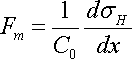
where C0 = no. of atoms per unit volume.
A conductor has along it, a segment of length, L, which has a raised atomic diffusivity. The material of the conductor develops damage when the difference in hydrostatic stress between the ends of such a segment reaches the value (ΔσH)crit. Derive the critical condition for the damage to develop in terms of L and current density, j, in the conductor. -
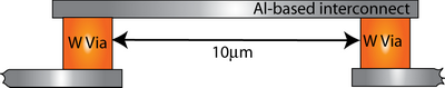
An IC has several levels of Al-based metallization linked by W vias. In a test, electromigration damage, develops in an Al-based conductor linking two vias when the current density flowing through it from one via to the other 10 μm away exceeds 9×10⁹ A m-2. It is planned to use the same materials with a current density of 1.2×10¹⁰ A m-2. What condition must be met by the length of links between vias for damage to be avoided? How will the temperature of the operation affect the development of electromigration damage?
-
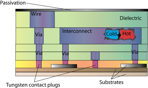
In the schematic diagram of a microelectronic device (below), where would electromigration-induced damage be observed? Give your reasons. What type of material would you use for the vias and interconnects, and why?
Going further
Books and Papers:
- Reliability and Failure of Electronic Materials and Devices by Milton Ohring, Academic Press, San Diego, 1998.
Provides a good overall explanation on the topic of electromigration
- Review Article: Electromigration in integrated circuit conductors by J R Lloyd (J. Phys. D: Appl. Phys. 32 (1999) R109-R118).
A good summary on electromigration in integrated circuit conductors
- VLSI Technology by S.M. Sze (editor), Mc-Graw-Hill Book Company, New Jersey, 1988.
Contains a good section on metallization and its choice of use for different materials
Website:
It contains a nice simple description of the electromigration process. Several other searches can be made within Wikipedia, the free encyclopedia, to look up technical terms.
Different parts of an integrated circuit
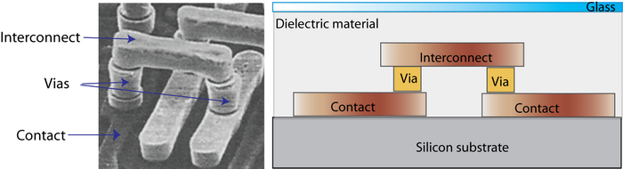
Scanning electron micrograph reprinted from ‘Reliability and Failure of Electronic Materials and Devices’ by Milton Ohring, Copyright 1998, with permission from Elsevier.
The metallic parts that electrically interconnect the various device structures on the silicon (Si) substrate are collectively known as metallization.
We can distinguish:
- contacts: metallization in direct contact with the Si substrate.
- vias: conducting paths between two or more metallization layers.
- interconnects: lines which connect the semiconductor components.
Most metallization lines are currently Al-based, for which electromigration-induced damage has been previously studied. There has been a technological advancement towards the use of Cu-based metallization, though most of the examples (within this TLP) are based mainly on Al-based metallization. Some references will be made later with regards to Cu-based lines.
All the metallization are protected in a closed system using an insulating material (called dielectric). The standard material used is SiO2 in layers, of which the top layer consists of glass. There is an increasing interest in using dielectrics of a lower dielectric constant than SiO2 – for example, some polymers.
Moore's Law

The increasing trend for the number of transistors on a chip has followed the prediction made by Moore’s Law.Data for this plot were obtained from Intel’s website.
Problems associated with the increase in resistance
-->The equations below show the interlinking relationships between resistance, capacitance, and resistor-capacitor (RC) delay with line width, L:
$$\displaylines{ {\rm{Resistance, }}R' = {{L\rho } \over A} = {{L\rho } \over {W{t_{metal}}}} \cr {\rm{Capacitance, }}C = \varepsilon {\varepsilon _0}{A \over d} = \varepsilon {\varepsilon _0}{{{t_{metal}}L} \over D} \cr {\rm{RC time delay }} = {\rm{ (}}R \times C) \propto {\rm{ }}\rho \varepsilon {\varepsilon _0}{{{L^2}} \over {WD}} \cr} $$
where: L = length of metallization line (m),
In the operation of an IC, it is therefore important that resistances of interconnects, vias and contacts remain within the range specified in the circuit design. Due to the effect it has on the RC time delay (see definition below), a change of resistance of 10% is enough to cause problems. In electromigration testing, a 10% change in resistance is often taken to represent “failure” (note how much less extreme an event this is compared to the formation of an open or short circuit).
The RC time delay is the major factor limiting device speed – also known as clock speed – the speed in which a microprocessor executes instructions. Therefore, the associated increase in resistance due to electromigration causes a longer RC time delay, resulting in slower clock speed, thus fewer instructions can be executed by the CPU per second.
Video showing hillock growth (wide metallization lines)
Video of hillock growth
Video showing void growth and migration (wide metallization lines)
Video of void growth
Video showing void growth (modern, narrow metallization lines)
Video of void growth
Blech length
The likelihood of electromigration damage depends not only on current density, but also on the absolute length of conducting segments. As shown by Blech, prevention of electromigration damage is possible when the product of the current density, j, and line length, l, is below a critical value (as shown below):
$${(jl)_c} = {{\Delta \sigma {\rm{ }}\Omega } \over {{Z^ * }e\rho }} $$
where Ω is the activation volume (m3) and σ is the hydrostatic component of the mechanical stress (kg m-1 s-2).
This relationship can be derived simply, by looking at the different contributions to flux within the metallization line. Electromigration of atoms, often results in a build up of stress within the metallization line. Regions of compressive and tensile stresses develop, resulting in a variation of stress (stress gradient) along the line. This stress gradient contributes to the gradient in the chemical potential, and thereby effects the mass flux, J:
$$J = {{DC} \over {RT}}\left( {{Z^ * }e\rho j - \Omega {{\Delta \sigma } \over {\Delta x}}} \right) $$
The animation below depicts the development of stress gradient during a Blech length experiment.
If the stress gradient is permitted to grow without the onset of damage (i.e. the stresses within the metallization line does not exceed the critical absolute stress levels for onset of damage), eventually its contribution to the chemical potential gradient is equal and opposite to that of the electric field. At that point, there is no gradient in chemical potential and no net flux of mass – thus the stress gradient does not continue to grow as it has achieved steady-state.$$\eqalign{ & {Z^ * }e\rho j = \Omega {{\Delta \sigma } \over {\Delta x}} \cr & {{\Delta \sigma } \over {\Delta x}} = {{{Z^ * }e\rho j} \over \Omega } \cr} $$
Therefore, can approximate to:
$$\eqalign{ & {{\Delta \sigma } \over l} = {{{Z^ * }e\rho j} \over \Omega } \cr & {(jl)_c} = {{\Delta \sigma {\rm{ }}\Omega } \over {{Z^ * }e\rho }} \cr} $$
There is no electromigration damage below (jlc). An estimation can therefore be made for the longest conductor, which would have “infinite” life.
Joule-heating effects
Joule heating refers to the increase in temperature of a conductor as a result of resistance to the electrical current flowing through it. At an atomic level, Joule-heating is the result of moving electrons colliding with atoms in a conductor, whereupon momentum is transferred to the atoms, increasing their kinetic energy in the form of heat.
Heat arising from Joule heating of the conductor causes the atoms to vibrate further from their ideal lattice positions, thereby increasing the electron scattering events. This is manifested as an increase in resistance, and acceleration in the process of electromigration.
High current density → Large number of scattered electrons → More electromigration
Temperature rises are normally small in ICs because the silicon substrate acts as a good heat sink.
Current crowding
Current crowding generates electromigration damage through the effects of Joule heating. This accelerating effect of raised temperature is observed once a void has started to form in the metallization line.
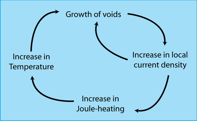
Growth of a void causes a reduction in cross-sectional area giving current crowding, i.e. an increase in current density and, therefore, an increase in local temperature. The temperature increase causes the local rate of atomic migration to increase, increasing flux divergences and accelerating the rate of electromigration damage. Accelerating void growth continues until the void is large enough to cause a significant problem within the IC, through increase of resistance, or ultimately, melting and the formation of an open circuit.
Data from Smithells Metals Reference Book
The relationship D =D0 exp(-Q/RT) is used to obtain the self diffusion of Al in Al and W in W.
D0 / m2 s-1
Q / kJ mol-1
W*
D1 = 0.04 × 10⁻⁴
D2 = 46 × 10-4Q1 = 526 ± 50
Q2 = 666 ± 59Al
1.71 × 10⁻⁴
142 ± 1
* The measured diffusivity of tungsten when plotted as lnD vs 1/T is curved and can be fitted by a sum of two terms: D = D1exp(Q1/RT) + D2exp(Q2/RT).
To obtain values for grain-boundary diffusion at 300 K, measured data have been extrapolated to give a relationship with the melting temperature, Tm, for:
FCC metals:
Dgb = 0.3 × 10⁻⁴ exp (-8.9 Tm/T) m2 s-1
Tm,Al = 933 K
Dgb,Al = 2.86 × 10⁻¹⁷ m2 s-1BCC metals:
Dgb = 1.84 × 10⁻⁵ exp (-10.4 Tm/T)
Tm,W = 3695 K
Dgb = 4.31 × 10-61 m2 s-1Note how W, having a much higher melting point, has a lower diffusivity than Al at a given temperature (in this case 300 K).
Equations obtained from ‘Fundamentals of Grain and Interphase Boundary Diffusion Third Edition’ by I. Kaur, Y. Mishin and W. Gus; Wiley, Chichester, 1995.
Academic consultant: Lindsay Greer (University of Cambridge)
Content development: Joo Ching Chua
Web development: Jin Chong TanThis DoITPoMS TLP was funded by the UK Centre for Materials Education and the Department of Materials Science and Metallurgy, University of Cambridge.