Different parts of an integrated circuit
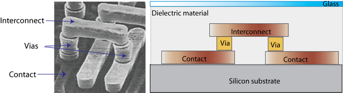
Scanning electron micrograph reprinted from ‘Reliability and Failure of Electronic Materials and Devices’ by Milton Ohring, Copyright 1998, with permission from Elsevier.
The metallic parts that electrically interconnect the various device structures on the silicon (Si) substrate are collectively known as metallization.
We can distinguish:
- contacts: metallization in direct contact with the Si substrate.
- vias: conducting paths between two or more metallization layers.
- interconnects: lines which connect the semiconductor components.
Most metallization lines are currently Al-based, for which electromigration-induced damage has been previously studied. There has been a technological advancement towards the use of Cu-based metallization, though most of the examples (within this TLP) are based mainly on Al-based metallization. Some references will be made later with regards to Cu-based lines.
All the metallization are protected in a closed system using an insulating material (called dielectric). The standard material used is SiO2 in layers, of which the top layer consists of glass. There is an increasing interest in using dielectrics of a lower dielectric constant than SiO2 – for example, some polymers.